Features: ♦ 1700MHz to 2200MHz RF Frequency Range
♦ 1900MHz to 2400MHz LO Frequency Range (MAX9996)
♦ 1400MHz to 2000MHz LO Frequency Range (MAX9994)
♦ 40MHz to 350MHz IF Frequency Range
♦ 8.3dB Conversion Gain
♦ +26.5dBm Input IP3
♦ +12.6dBm Input 1dB Compression Point
♦ 9.7dB Noise Figure
♦ 72dBc 2LO-2RF Spurious Rejection at PRF = -10dBm
♦ Integrated LO Buffer
♦ Integrated RF and LO Baluns for Single-Ended Inputs
♦ Low -3dBm to +3dBm LO Drive
♦ Built-In SPDT LO Switch with 43dB LO1 to LO2 Isolation and 50ns Switching Time
♦ Pin Compatible with MAX9984/MAX9986 815MHz to 995MHz Mixers
♦ Functionally Compatible with MAX9993
♦ External Current-Setting Resistors Provide Option for Operating Mixer in Reduced
Power/ Reduced erformance Mode
♦ Lead-Free Package AvailableApplicationUMTS/WCDMA Base Stations
DCS1800/PCS1900 EDGE Base Stations
cdmaOne™ and cdma2000® Base Stations
PHS/PAS Base Stations
Predistortion Receivers
Fixed Broadband Wireless Access
Wireless Local Loop
Private Mobile Radios
Military Systems
Microwave Links
Digital and Spread-Spectrum Communication
Systems
cdma2000 is a registered trademark of Telecommunications Industry Association.
cdmaOne is a trademark of CDMA Development Group.Pinout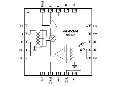 Specifications
Vcc to GND...........................................................-0.3V to +5.5V
IF+, IF-, LOBIAS, LOSEL, IFBIAS to GND......-0.3V to (Vcc + 0.3V)
TAP........................................................................-0.3V to +1.4V
LO1, LO2, LEXT to GND..........................................-0.3V to +0.3V
RF, LO1, LO2 Input Power ..............................................+12dBm
RF (RF is DC shorted to GND through a balun) ...................50mA
Continuous Power Dissipation (TA = +70°C)
20-Pin Thin QFN-EP (derate 26.3mW/°C above +70°C).....2.1W
JA ................................................................................+38°C/W
JC ................................................................................+13°C/W
Operating Temperature Range (Note A) ....TC = -40°C to +85°C
Junction Temperature........................................................+150°C
Storage Temperature Range .............................-65°C to +150°C
Lead Temperature (soldering, 10s) ...................................+300°C
Stresses beyond those listed under "Absolute Maximum Ratings" may cause permanent damage to the device. These are stress ratings only, and functional operation of the device at these or any other conditions beyond those indicated in the operational sections of the specifications is not implied. Exposure to absolute maximum rating conditions for extended periods may affect device reliability.
Note A: TC is the temperature on the exposed paddle of the package
DescriptionThe MAX9996 high-linearity downconversion mixer provides 8.3dB gain, +26.5dBm IIP3, and 9.7dB NF for 1700MHz to 2200MHz UMTS/WCDMA, DCS, and PCS base-station receiver applications. With a 1900MHz to 2400MHz LO requency range, this particular mixer is ideal for high-side LO injection receiver architectures. Low-side LO injection is supported by the MAX9994, which is pin-for-pin and functionally compatible with the MAX9996.
In addition to offering excellent linearity and noise performance, the MAX9996 also yields a high level of component integration. This device includes a doublebalanced passive mixer core, an IF amplifier, a dualinput LO selectable switch, and an LO buffer. On-chip baluns are also integrated to allow for single-ended RF and LO inputs. The MAX9996 requires a nominal LO drive of 0dBm, and supply current is guaranteed to be below 240mA.
The MAX9994/MAX9996 are pin compatible with the MAX9984/MAX9986 815MHz to 995MHz mixers, making this entire family of downconverters ideal for applications where a common PC board layout is used for both frequency bands. The MAX9996 is also functionally compatible with the MAX9993.
The MAX9996 is available in a compact, 20-pin, thin QFN package (5mm x 5mm) with an exposed paddle. Electrical performance is guaranteed over the extended -40°C to +85°C temperature range.

 MAX9996 Data Sheet