MBC13720

ApplicationThe MBC13720 SiGe:C LNA is designed for applications in the 400 MHz to 2.4 GHz range. It has four different modes; Low IP3, High IP3, Bypass, and Standby. The IC is programmable through the Enable 1 and 2 pins. In Low IP3 mode, the current consumption is optimized. Current consumption i...

product image

MBC13720 Picture
SeekIC No. : 004413998 Detail

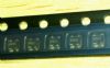
MBC13720: ApplicationThe MBC13720 SiGe:C LNA is designed for applications in the 400 MHz to 2.4 GHz range. It has four different modes; Low IP3, High IP3, Bypass, and Standby. The IC is programmable through t...

floor Price/Ceiling Price

Part Number:
MBC13720
Supply Ability:
5000

Price Break

  • Qty
  • 1~5000
  • Unit Price
  • Negotiable
  • Processing time
  • 15 Days
Total Cost: $ 0.00

SeekIC Buyer Protection PLUS - newly updated for 2013!

  • Escrow Protection.
  • Guaranteed refunds.
  • Secure payments.
  • Learn more >>

Month Sales

268 Transactions

Rating

evaluate  (4.8 stars)

Upload time: 2024/5/1

Payment Methods

All payment methods are secure and covered by SeekIC Buyer Protection PLUS.

Notice: When you place an order, your payment is made to SeekIC and not to your seller. SeekIC only pays the seller after confirming you have received your order. We will also never share your payment details with your seller.
Product Details

Description


Application

The MBC13720 SiGe:C LNA is designed for applications in the 400 MHz to 2.4 GHz range. It has four different modes; Low IP3, High IP3, Bypass, and Standby. The IC is programmable through the Enable 1 and 2 pins. In Low IP3 mode, the current consumption is optimized. Current consumption is higher in High IP3 mode to boost the intercept point performance. The gain difference between Low IP3 and High IP3 modes is typically 1.0 dB and typically the Low IP3 mode has a slightly better noise figure performance.

The internal bypass switch is designed for broadband applications. One of the advantages of the MBC13720 is the simplification of matching network in both bypass and amplifier modes. The bypass switch is designed such that the changes of input and output return losses between bypass mode and amplifier mode is minimized. As a result, the mismatch at the LNA input and output is minimized and therefore, the matching network design is simplified as well.

In the design of the external matching network, conjugate match condition does not necessarily provide the best noise figure performance. Balancing between noise figure, gain, and intercept point is the major design consideration. Typical circuits are provided in Figures 2 and 3 for 1.9 GHz, 2.4 GHz and 900 MHz applications.

In Figure 2, it shows the typical application circuit at 1.9 and 2.4 GHz. The noise figure, input intercept point, gain, and return losses are optimized. L2 and C2 act as a low frequency trap to improve the input intercept point. The noise figure measured on this board is 1.4 dB (in Low IP3 mode) at 1.9 GHz, including the external components, connectors, and PC board. The input third order intercept point is 10 dBm (in High IP3 mode).


Specifications

Ratings Symbol Value Unit
Supply Voltage VCC 3.3 V
Storage Temperature Range Tstg -65 to 150 °C
Operating Ambient Temperature Range TA -30 to 85 °C
NOTES: 1. Maximum Ratings are those values beyond which damage to the device may occur.
             Functional operation should be restricted to the limits in the Recommended Operating
             Conditions and Electrical Characteristics tables.
             2. ESD (electrostatic discharge) immunity meets Human Body Model (HBM) 550 V and
               Machine Model (MM) 50 V. Additional EST data available upon request.


Customers Who Bought This Item Also Bought

Margin,quality,low-cost products with low minimum orders. Secure your online payments with SeekIC Buyer Protection.
Inductors, Coils, Chokes
Crystals and Oscillators
Potentiometers, Variable Resistors
Audio Products
View more