Features: • 0.33 mm Process Technology
• Simultaneous Read/Write operations (dual bank)
Multiple devices available with different bank sizes (Refer to Table 1)
Host system can program or erase in one bank, then immediately and simultaneously read from the other bank
Zero latency between read and write operations
Read-while-erase
Read-while-program
• Single 3.0 V read, program, and erase
Minimizes system level power requirements
• Compatible with JEDEC-standard commands
Uses same software commands as E2PROMs
• Compatible with JEDEC-standard world-wide pinouts
48-pin TSOP(I) (Package suffix: PFTN Normal Bend Type, PFTR Reversed Bend Type)
48-ball FBGA (Package suffix: PBT)
• Minimum 100,000 program/erase cycles
• High performance
70 ns maximum access time
• Sector erase architecture
Eight 4K word and thirty one 32K word sectors in word mode
Eight 8K byte and thirty one 64K byte sectors in byte mode
Any combination of sectors can be concurrently erased. Also supports full chip erase.
• Boot Code Sector Architecture
T = Top sector
B = Bottom sector
• Hidden ROM (Hi-ROM) region
64K byte of Hi-ROM, accessible through a new "Hi-ROM Enable" command sequence
Factory serialized and protected to provide a secure electronic serial number (ESN)
• WP/ACC input pin
At VIL, allows protection of boot sectors, regardless of sector protection/unprotection status
At VIH, allows removal of boot sector protection
At VACC, increases program performance
• Embedded EraseTM Algorithms
Automatically pre-programs and erases the chip or any sector
• Embedded ProgramTM Algorithms
Automatically writes and verifies data at specified address
• Data Polling and Toggle Bit feature for detection of program or erase cycle completion
• Ready/Busy output (RY/ YB)
Hardware method for detection of program or erase cycle completion
• Automatic sleep mode
When addresses remain stable, automatically switch themselves to low power mode.
• Low VCC write inhibit2.5 V
• Erase Suspend/Resume
Suspends the erase operation to allow a read data and/or program in another sector within the same device
• Sector group protection
Hardware method disables any combination of sector groups from program or erase operations
• Sector Group Protection Set function by Extended sector group protection command
• Fast Programming Function by Extended Command
• Temporary sector group unprotection
Temporary sector group unprotection via the RESET pin.
• In accordance with CFI (Common Flash Memory Interface)Pinout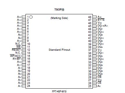 Specifications
| Parameter |
Symbol |
Conditions |
Rating |
Unit |
| Min. |
Max. |
| Storage Temperature |
Tstg |
- |
55 |
+125 |
°C |
Ambient Temperature with
Power Applied |
TA |
- |
40 |
+85 |
°C |
Voltage with respect to
Ground All pins except A9,
OE, RESET (Note 1) |
VIN, VOUT |
- |
0.5 |
VCC+0.5 |
V |
Power Supply Voltage
(Note 1) |
VCC |
- |
0.5 |
+4.0 |
V |
| A9, OE, and RESET(Note 2) |
VIN |
- |
0.5 |
+13.0 |
V |
| WP/ACC (Note 3) |
VIN |
- |
0.5 |
+10.5 |
V |
WARNING: Semiconductor devices can be permanently damaged by application of stress (voltage, current,
temperature, etc.) in excess of absolute maximum ratings. Do not exceed these ratings.
Notes: 1. Minimum DC voltage on input or I/O pins are 0.5 V. During voltage transitions, inputs may negative
overshoot VSS to 2.0 V for periods of up to 20 ns. Maximum DC voltage on output and I/O pins are VCC
+0.5 V. During voltage transitions, outputs may positive overshoot to VCC +2.0 V for periods of up to 20 ns.
2. Minimum DC input voltage on A9, OE and RESET pins are 0.5 V. During voltage transitions, A9, OE
and RESETpins may negative overshoot VSS to 2.0 V for periods of up to 20 ns. Maximum DC input
voltage on A9,OE andRESET pins are +13.0 V which may positive overshoot to 14.0 V for periods of
up to 20 ns. when VCC is applied.
3. Minimum DC input voltage on WP/ACC pin is 0.5 V. During voltage transitions, WP/ACC pin may
negative overshoot VSS to 2.0 V for periods of up to 20 ns. Maximum DC input voltage on WP/ACC pin
iis when Vcc is applied.DescriptionThe MBM29DL16XTD/BD are a 16M-bit, 3.0 V-only Flash memory organized as 2M bytes of 8 bits each or 1M words of 16 bits each. The MBM29DL16XTD/BD are offered in a 48-pin TSOP(I) and 48-ball FBGA Package.
These devices are designed to be programmed in-system with the standard system 3.0 V VCC supply. 12.0 V VPP and 5.0 V VCC are not required for write or erase operations. The devices can also be reprogrammed in standard EPROM programmers.
MBM29DL16XTD/BD are organized into two banks, Bank 1 and Bank 2, which can be considered to be two separate memory arrays as far as certain operations are concerned. These devices are the same as Fujitsu's standard 3 V only Flash memories with the additional capability of allowing a normal non-delayed read access from a non-busy bank of the array while an embedded write (either a program or an erase) operation is simultaneously taking place on the other bank.
In the MBM29DL16XTD/BD, a new design concept is implemented, so called "Sliding Bank Architecture". Under this concept, the MBM29DL16XTD/BD can be produced a series of devices with different Bank 1/Bank 2 size combinations; 0.5 Mb/15.5 Mb, 2 Mb/14 Mb, 4 Mb/12 Mb, 8 Mb/8 Mb.
The standard MBM29DL16XTD/BD offer access times 70 ns, 90 ns and 120 ns, allowing operation of high-speed microprocessors without wait states. To eliminate bus contention the devices have separate chip enable (CE), write enable (WE), and output enable (OE) controls.
The MBM29DL16XTD/BD are pin and command set compatible with JEDEC standard E2PROMs. Commands are written to the command register using standard microprocessor write timings. Register contents serve as input to an internal state-machine which controls the erase and programming circuitry. Write cycles also internally latch addresses and data needed for the programming and erase operations. Reading data out of the devices is similar to reading from 5.0 V and 12.0 V Flash or EPROM devices.
The MBM29DL16XTD/BD are programmed by executing the program command sequence. This will invoke the Embedded Program Algorithm which is an internal algorithm that automatically times the program pulse widths and verifies proper cell margin. Typically, each sector can be programmed and verified in about 0.5 seconds. Erase is accomplished by executing the erase command sequence. This will invoke the Embedded Erase Algorithm which is an internal algorithm that automatically preprograms the array if it is not already programmed before executing the erase operation. During erase, the devices automatically time the erase pulse widths and verify proper cell margin.
A sector is typically erased and verified in 1.0 second. (If already completely preprogrammed.)
The devices also feature a sector erase architecture. The sector mode allows each sector to be erased and reprogrammed without affecting other sectors. The MBM29DL16XTD/BD are erased when shipped from the factory.
The devices feature single 3.0 V power supply operation for both read and write functions. Internally generated and regulated voltages are provided for the program and erase operations. A low VCC detector automatically inhibits write operations on the loss of power. The end of program or erase is detected by Eata Polling of DQ7, by the Toggle Bit feature on DQ6, or the RY/BY output pin. Once the end of a program or erase cycle has been completed, the devices internally reset to the read mode.
Fujitsu's Flash technology combines years of EPROM and E2PROM experience to produce the highest levels of quality, reliability, and cost effectiveness. The MBM29DL16XTD/BD memories electrically erase the entire chip or all bits within a sector simultaneously via Fowler-Nordhiem tunneling. The bytes/words are programmed one byte/word at a time using the EPROM programming mechanism of hot electron injection.

 MBM29DL16XTD Data Sheet