Features: • Single 5.0 V read, write, and erase Minimizes system level power requirements
• Compatible with JEDEC-standard commands Pinout and software compatible with single-power supply Flash Superior inadvertent write protection
• 48-pin TSOP(I) (Package Suffix: PFTN-Normal Bend Type, PFTR-Reverse Bend Type)
• Minimum 100,000 write/erase cycles
• High performance 70 ns maximum access time
• Sector erase architecture Uniform sectors of 64 K bytes each Any combination of sectors can be erased. Also supports full chip erase.
• Embedded Erase™ Algorithms Automatically pre-programs and erases the chip or any sector
• Embedded Program™ Algorithms Automatically programs and verifies data at specified address
• Data Polling and Toggle Bit feature for detection of program or erase cycle completion
• Ready/Busy output (RY/BY) Hardware method for detection of program or erase cycle completion
• Low VCC write inhibit £ 3.2 V
• Hardware RESET pin Resets internal state machine to the read mode
• Erase Suspend/Resume Supports reading or programming data to a sector not being erased
• Sector group protection Hardware method that disables any combination of sector groups from write or erase operation (a sector group consists of 4 adjacent sectors of 64 K bytes each)
• Temporary sector groups unprotection Temporary sector unprotection via the RESET pin
Pinout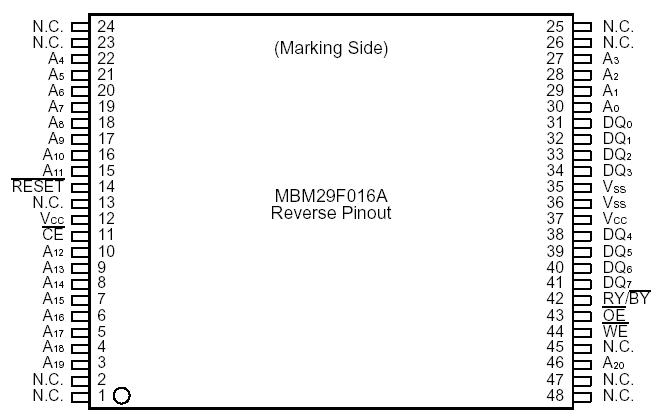 SpecificationsStorage Temperature ................................................................................55°C to +125°C
Ambient Temperature with Power Applied ................................................. 40°C to +85°C
Voltage with Respect to Ground All pins except A9, OE, and RESET (Note 1).2.0 V to +7.0 V
VCC (Note 1) .................................................................................................2.0 V to +7.0 V
A9, OE, and RESET (Note 2) ........................................................................2.0 V to +13.5 VDescriptionThe MBM29F016A-70 is a 16 M-bit, 5.0 V-Only Flash memory organized as 2 M bytes of 8 bits each. The 2 M bytes of data is divided into 32 sectors of 64 K bytes for flexible erase capability. The 8 bit of data will appear on DQ0 to DQ7. The MBM29F016A is offered in a 48-pin TSOP(I) package. This device is designed to be programmed in-system with the standard system 5.0 V VCC supply. A 12.0 V VPP is not required for program or erase operations. The device can also be reprogrammed in standard EPROM programmers. The standard MBM29F016A offers access times between 70 ns and 120 ns allowing operation of high-speed microprocessors without wait states. To eliminate bus contention the device has separate chip enable (CE), write enable (WE), and output enable (OE) controls.
The MBM29F016A-70 is command set compatible with JEDEC standard E2PROMs. Commands are written to the command register using standard microprocessor write timings. Register contents serve as input to an internal state-machine which controls the erase and programming circuitry. Write cycles also internally latch addresses and data needed for the programming and erase operations. Reading data out of the device is similar to reading from 12.0 V Flash or EPROM devices. The MBM29F016A is programmed by executing the program command sequence. This will invoke the Embedded Program Algorithm which is an internal algorithm that automatically times the program pulse widths and verifies proper cell margin. Each sector can be programmed and verified in less than 0.5 seconds. Erase is accomplished by executing the erase command sequence. This will invoke the Embedded Erase Algorithm which is an internal algorithm that automatically preprograms the array if it is not already programmed before executing the erase operation. During erase, the device automatically times the erase pulse widths and verifies proper cell margin. This device also features a sector erase architecture. The sector erase mode allows for sectors of memory to be erased and reprogrammed without affecting other sectors. A sector is typically erased and verified within 1 second (if already completely preprogrammed). The MBM29F016A is erased when shipped from the factory.
The MBM29F016A-70 device also features hardware sector group protection. This feature will disable both program and erase operations in any combination of eight sector groups of memory. A sector group consists of four adjacent sectors grouped in the following pattern: sectors 0-3, 4-7, 8-11, 12-15, 16-19, 20-23, 24-27, and 28-31. Fujitsu has implemented an Erase Suspend feature that enables the user to put erase on hold for any period of time to read data from or program data to a non-busy sector. Thus, true background erase can be achieved. The device features single 5.0 V power supply operation for both read and program functions. Internally generated and regulated voltages are provided for the program and erase operations. A low VCC detector automatically inhibits write operations during power transitions. The end of program or erase is detected by Data Polling of DQ7, or by the Toggle Bit I feature on DQ6 or RY/BY output pin. Once the end of a program or erase cycle has been completed, the device automatically resets to the read mode.
The MBM29F016A-70 also has a hardware RESET pin. When this pin is driven low, execution of any Embedded Program or Embedded Erase operations will be terminated. The internal state machine will then be reset into the read mode. The RESET pin may be tied to the system reset circuity. Therefore, if a system reset occurs during the Embedded Program or Embedded Erase operation, the device will be automatically reset to a read mode. This will enable the system microprocessor to read the boot-up firmware from the Flash memory. Fujitsu's Flash technology combines years of EPROM and E2PROM experience to produce the highest levels of quality, reliability, and cost effectiveness. The MBM29F016A memory electrically erases all bits within a sector simultaneously via Fowler-Nordheim tunneling. The bytes are programmed one byte at a time using the EPROM programming mechanism of hot electron injection.

 MBM29F016A-70 Data Sheet