Features: • Single 5.0 V read, write, and erase Minimizes system level power requirements
• Compatible with JEDEC-standard commands Pinout and software compatible with single-power supply Flash Superior inadvertent write protection
• 48-pin TSOP(I) (Package Suffix: PFTN-Normal Bend Type, PFTR-Reverse Bend Type) 40-pin TSOP(I) (Package Suffix: PTN-Normal Bend Type, PTR-Reversed Bend Type) 44-pin SOP (Package Suffix: PF)
• Minimum 100,000 write/erase cycles
• High performance 55 ns maximum access time
• Sector erase architecture Uniform sectors of 64 K bytes each Any combination of sectors can be erased. Also sup-ports full chip erase.
• Embedded Erase™ Algorithms Automatically pre-programs and erases the chip or any sector
• Embedded Program™ Algorithms Automatically programs and verifies data at specified address
•Data Polling and Toggle Bit feature for detection of program or erase cycle completion
• Ready/Busy output (RY/BY) Hardware method for detection of program or erase cycle completion
•Low VCC write inhibit 3.2 V
• Hardware RESET pin Resets internal state machine to the read mode
• Erase Suspend/Resume Supports reading or programming data to a sector not being erased
• Sector group protection Hardware method that disables any combination of sector groups from write or erase operation (a sector group consists of 2 adjacent sectors of 64 K bytes each)
• Temporary sector groups unprotection Temporary sector unprotection via the RESET pinPinout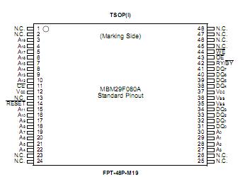 SpecificationsStorage Temperature .....................................................................................55°C to +125°C
Ambient Temperature with Power Applied ........................................................40°C to +85°C
Voltage with Respect to Ground All pins except A9, OE, and RESET (Note 1).......2.0 V to +7.0 V
VCC (Note 1) .......................................................................................................2.0 V to +7.0 V
A9, OE, and RESET (Note 2) ..............................................................................2.0 V to +13.5 VDescriptionThe MBM29F080A-90 is a 8 M-bit, 5.0 V-Only Flash memory organized as 1 M bytes of 8 bits each. The 1 M bytes of data is divided into 16 sectors of 64 K bytes for flexible erase capability. The 8 bit of data will appear on DQ0 to DQ7. The MBM29F080A is offered in a 48-pin TSOP(I), 40-pin TSOP, and 44-pin SOP packages. This device is designed to be pro-grammed in-system with the standard system 5.0 V VCC supply. A 12.0 V VPP is not required for program or erase operations. The device can also be reprogrammed in standard EPROM programmers.
The standard MBM29F080A-90 offers access times between 55 ns and 90 ns allowing operation of high-speed micro-processors without wait states. To eliminate bus contention the device has separate chip enable (CE), write enable (WE), and output enable (OE) controls.
The MBM29F080A-90 is command set compatible with JEDEC standard E2PROMs. Commands are written to the command register using standard microprocessor write timings. Register contents serve as input to an internal state-machine which controls the erase and programming circuitry. Write cycles also internally latch addresses and data needed for the programming and erase operations. Reading data out of the device is similar to reading from 12.0 V Flash or EPROM devices.
The MBM29F080A-90 is programmed by executing the program command sequence. This will invoke the Embedded Pro-gram Algorithm which is an internal algorithm that automatically times the program pulse widths and verifies proper cell margin. Each sector can be programmed and verified in less than 0.5 seconds. Erase is accomplished by executing the erase command sequence. This will invoke the Embedded Erase Algorithm which is an internal algorithm that automatically preprograms the array if it is not already programmed before executing the erase operation. During erase, the device automatically times the erase pulse widths and verifies proper cell margin.

 MBM29F080A-90 Data Sheet