Features: • Single 3.0 V read, program, and erase Minimizes system level power requirements
• Compatible with JEDEC-standard commands Uses same software commands as E2PROMs
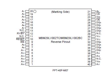
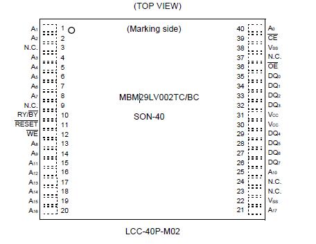
• Compatible with JEDEC-standard world-wide pinouts
40-pin TSOP(I) (Package suffix: PTN Normal Bend Type, PTR Reversed Bend Type)
40-pin SON (Package suffix: PNS)
• Minimum 100,000 program/erase cycles
• High performance
70 ns maximum access time
• Sector erase architecture
One 16K byte, two 8K bytes, one 32K byte, and three 64K bytes
Any combination of sectors can be concurrently erased. Also supports full chip erase
• Boot Code Sector Architecture
T = Top sector
B = Bottom sector
• Embedded EraseTM Algorithms
Automatically pre-programs and erases the chip or any sector
• Embedded ProgramTM Algorithms
Automatically writes and verifies data at specified address
• Data Polling and Toggle Bit feature for detection of program or erase cycle completion
• Ready/Busy output (RY/BY)
Hardware method for detection of program or erase cycle completion
• Automatic sleep mode
When addresses remain stable, automatically switch themselves to low power mode
• Low VCC write inhibit 2.5 V
• Erase Suspend/Resume
Suspends the erase operation to allow a read data in another sector within the same device
• Sector protection
Hardware method disables any combination of sectors from program or erase operations
• Sector Protection Set function by Extended sector protection command
• Temporary sector unprotection
Temporary sector unprotection via the RESET pinPinout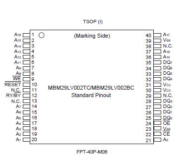
 SpecificationsStorage Temperature ..................................................................................................55 to +125
Ambient Temperature with Power Applied .............................................................. ......40 to +85
Voltage with respect to Ground All pins except A9, OE and RESET (Note 1) ..........0.5 V to VCC+0.5 V
VCC (Note 1) ................................................................................................................0.5 V to +5.5 V
A9, OE, and RESET (Note 2) ................................................................................ ......0.5 V to +13.0 VDescriptionThe MBM29LV002BC are a 2M-bit, 3.0 V-only Flash memory organized as 256K bytes of 8 bits each. The MBM29LV002TC/BC are offered in a 40-pin TSOP(I) and 40-pin SON packages. These devices are designed to be programmed in-system with the standard system 3.0 V V
CC supply. 12.0 V VPP and 5.0 V V
CC are not required for write or erase operations. The devices can also be reprogrammed in standard EPROM programmers.
The standard MBM29LV002BC offer access times 70 ns and 120 ns, allowing operation of high-speed microprocessors without wait states. To eliminate bus contention the devices have separate chip enable (CE),write enable (WE), and output enable (OE) controls.
The MBM29LV002BC are pin and command set compatible with JEDEC standard E2PROMs. Commands are written to the command register using standard microprocessor write timings. Register contents serve as input to an internal state-machine which controls the erase and programming circuitry. Write cycles also internally latch addresses and data needed for the programming and erase operations. Reading data out of the devices is similar to reading from 5.0 V and 12.0 V Flash or EPROM devices.
The MBM29LV002BC are programmed by executing the program command sequence. This will invoke the Embedded Program Algorithm which is an internal algorithm that automatically times the program pulse widths and verifies proper cell margin. Typically, each sector can be programmed and verified in about 0.5 seconds.
Erase is accomplished by executing the erase command sequence. This will invoke the Embedded Erase Algorithm which is an internal algorithm that automatically preprograms the array if it is not already programmed before executing the erase operation. During erase, the devices automatically time the erase pulse widths and verify proper cell margin.
Any individual sector is typically erased and verified in 1.0 second. (If already completely preprogrammed.) The devices also feature a sector erase architecture. The sector mode allows each sector to be erased and reprogrammed without affecting other sectors. The MBM29LV002TC/BC are erased when shipped from the factory.
MBM29LV002BC feature single 3.0 V power supply operation for both read and write functions. Internally generated and regulated voltages are provided for the program and erase operations. A low V
CC detector automatically inhibits write operations on the loss of power. The end of program or erase is detected by Data Polling of DQ
7, by the Toggle Bit feature on DQ
6, or the RY/BY output pin. Once the end of a program or erase cycle has been completed, the devices internally reset to the read mode.
Fujitsu's Flash technology combines years of EPROM and E2PROM experience to produce the highest levels of quality, reliability, and cost effectiveness. The MBM29LV002BC memories electrically erase the entire chip or all bits within a sector simultaneously via Fowler-Nordhiem tunneling. The bytes are programmed one byte at a time using the EPROM programming mechanism of hot electron injection.

 MBM29LV002BC Data Sheet