MC10

PinoutDescriptionThe MC10/100EL34 is a low skew ÷2, ÷4, ÷8 clock generation chip designed explicitly for low skew clock generation applications. The internal dividers are synchronous to each other, therefore, the common output edges are all precisely aligned. The MC10 can be driven by either a dif...

product image

MC10 Picture
SeekIC No. : 004414679 Detail

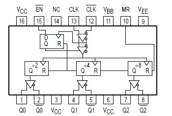
MC10: PinoutDescriptionThe MC10/100EL34 is a low skew ÷2, ÷4, ÷8 clock generation chip designed explicitly for low skew clock generation applications. The internal dividers are synchronous to each other, ...

floor Price/Ceiling Price

Part Number:
MC10
Supply Ability:
5000

Price Break

  • Qty
  • 1~5000
  • Unit Price
  • Negotiable
  • Processing time
  • 15 Days
Total Cost: $ 0.00

SeekIC Buyer Protection PLUS - newly updated for 2013!

  • Escrow Protection.
  • Guaranteed refunds.
  • Secure payments.
  • Learn more >>

Month Sales

268 Transactions

Rating

evaluate  (4.8 stars)

Upload time: 2024/4/24

Payment Methods

All payment methods are secure and covered by SeekIC Buyer Protection PLUS.

Notice: When you place an order, your payment is made to SeekIC and not to your seller. SeekIC only pays the seller after confirming you have received your order. We will also never share your payment details with your seller.
Product Details

Description


Pinout

  Connection Diagram


Description

The MC10/100EL34 is a low skew ÷2, ÷4, ÷8 clock generation chip designed explicitly for low skew clock generation applications. The internal dividers are synchronous to each other, therefore, the common output edges are all precisely aligned. The MC10 can be driven by either a differential or single-ended ECL or, if positive power supplies are used, PECL input signal. In addition, by using the VBB output, a sinusoidal source can be AC coupled into the device (see Interfacing section of the ECLinPSE Data Book DL140/D). If a single-ended input is to be used, the VBB output should be connected to the CLK input and bypassed to ground via a 0.01mF capacitor. The VBB output is designed to act as the switching reference for the input of the EL34 under single-ended input conditions, as a result, this pin can only source/sink up to 0.5mA of current.

The common enable (EN) is synchronous so that the internal dividers will only be enabled/disabled when the internal clock is already in the LOW state. This avoids any chance of generating a runt clock pulse on the internal clock when the MC10 is enabled/disabled as can happen with an asynchronous control. An internal runt pulse could lead to losing synchronization between the internal divider stages. The internal enable flip-flop is clocked on the falling edge of the input clock, therefore, all associated specification limits are referenced to the negative edge of the clock input.

Upon startup, the internal flip-flops will attain a random state; the master reset (MR) input allows for the synchronization of the internal dividers, as well as multiple EL34s in a system.


Customers Who Bought This Item Also Bought

Margin,quality,low-cost products with low minimum orders. Secure your online payments with SeekIC Buyer Protection.
Cables, Wires - Management
Undefined Category
Integrated Circuits (ICs)
Power Supplies - Board Mount
Computers, Office - Components, Accessories
Discrete Semiconductor Products
View more