Series: -
Mounting Type: Surface Mount
Current - Peak Output: 3A
Type: Low Side
Operating Temperature: -40°C ~ 125°C
Current - Output / Channel: 500mA
Number of Outputs: 8
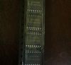
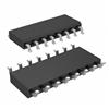
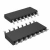
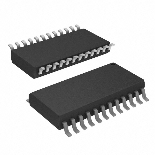
Package / Case: 24-SOIC (0.295", 7.50mm Width)
Supplier Device Package: 24-SOIC W
On-State Resistance: 600 mOhm
Input Type: SPI
Packaging: Cut Tape (CT)
Manufacturer: Freescale Semiconductor
Voltage - Supply: 9 V ~ 26.5 V
DescriptionThe MC33291DWR2 is designed as an eight output, low side power switch with 8-bit serial input control which is a versatile circuit designed for automotive applications, but is well suited for other environments.
MC33291DWR2 has seven features. (1)Designed to operate over wide supply voltages of 5.5 to 26.5V. (2)Interfaces to microprocessor using 8bit SPI I/O protocol up to 3.0MHz. (3)1.0A peak current outputs with maximum Rds(on) of 1.6 at Tj=150°C. (4)Outputs current limited to accommodate in-rush currents associated with switching incandescent loads. (5)Output voltages clamped to 53V during inductive switching. (6)Maximum sleep current (IPWR) of 25A. (7)Maximum of 4.0mA Idd during operation. Those are all the main features.
Some absolute maximum ratings of MC33291DWR2 have been concluded into several points as follow. (1)Its power supply voltage would be from -1.5V to 26.5V for nomal operation and would be from -13V to 60V for transient conditions. (2)Its logic supply voltage would be from -0.3V to 7.0V. (3)Its input pin voltage would be from -0.3V to 7.0V. (4)Its output clamp voltage would be from 45V to 65V. (5)Its output self-limit current would be from 1.0A ro 3.0A. (6)Its continuous per output current would be 500mA. (7)Its ESD voltage would be 2000V for human body model and would be 200V for machine model. (8)Its output clamp energy would be 50mJ. (9)Its recommended frequency of SPI operation would be 3.0MHz. (10)Its storage temperature range would be from -55°C to 150°C. (11)Its operating case temperature range would be from -40°C to 125°C. (12)Its power dissipation would be 2.0W. (13)Its soldering temperature would be 260°C. (14)Its thermal resistance would be 45°C/W for all outputs on and would be 60°C/W for single output on. It should be noted that stresses above those listed in absolute maximum ratings may cause permanent damage to device. Maximum output clamp energy capability at 150°C junction temperature using a single non-repetitive pulse method. And so on. If you have any question or suggestion or want to know more information about MC33291DWR2 please contact us for details. Thank you!
 MC33291DWR2 Data Sheet