Features: • Fast Switching and Propagation Speeds
• Low Crosstalk Between Switches
• Diode Protection on All Inputs/Outputs
• Analog Power Supply Range (VCC VEE) = 2.0 to 12.0 V
• Digital (Control) Power Supply Range (VCC GND) = 2.0 to 6.0 V
• Improved Linearity and Lower ON Resistance Than MetalGate Counterparts
• Low Noise
• In Compliance With the Requirements of JEDEC Standard No. 7A
• Chip Complexity: HC4051 - 184 FETs or 46 Equivalent Gates
HC4052 - 168 FETs or 42 Equivalent Gates
HC4053 - 156 FETs or 39 Equivalent GatesApplicationThe Channel Select and Enable control pins should be at VCC or GND logic levels. VCC being recognized as a logic high and GND being recognized as a logic low. In this example:
VCC = +5V = logic high
GND = 0V = logic low
The maximum analog voltage swings are determined by the supply voltages VCC and VEE. The positive peak analog
voltage should not exceed VCC. Similarly, the negative peak analog voltage should not go below VEE. In this example, the difference between VCC and VEE is ten volts. Therefore, using the configuration of Figure 15, a maximum analog signal of ten volts peaktopeak can be controlled. Unused analog inputs/outputs may be left floating (i.e., not connected). However, tying unused analog inputs and outputs to VCC or GND through a low value resistor helps minimize crosstalk and feedthrough noise that may be picked up by an unused switch.
Although used here, balanced supplies are not a requirement. The only constraints on the power supplies are that:
VCC GND = 2 to 6 volts
VEE GND = 0 to 6 volts
VCC VEE = 2 to 12 volts
and VEE GND
When voltage transients above VCC and/or below VEE are anticipated on the analog channels, external Germanium or Schottky diodes (Dx) are recommended as shown in Figure 16. These diodes should be able to absorb the maximum anticipated current surges during clipping.
Pinout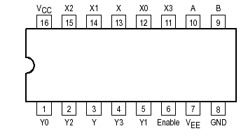 Specifications
|
Symbol |
Parameter |
Value |
Unit |
|
VCC |
Positive DC Supply Voltage (Referenced to GND)
(Referenced to GND) |
|
V |
|
VEE |
Negative Dc Supply Voltage (Referenced to GND) |
7.0 to VCC +0.5 |
V |
|
VIS |
Anaolg Input Voltage |
VEE 0.5 to
VCC + 0.5
|
V |
|
Iin |
Digital Input (Referenced to GND) |
0.5 to VCC + 0.5 |
|
|
|
DC Curent,Intl or Out of Any Pin |
± 25 |
mA |
|
PD |
Power Dissipation in Still Air, Plastic or Ceramic DIP†
SOIC Package†
TSSOP Package† |
750
500
450 |
mW |
|
Tstg |
Storage Temperature Range |
65 to + 150 |
|
|
TL |
Lead Temperature, 1 mm from Case for 10 Seconds
(Plastic DIP, SOIC or TSSOP Package)
(Ceramic DIP)
|
260
300 |
|
*Maximum Ratings are those values beyond which damage to the device may occur.Functional operation
should be restricted to the Recommended Operating Conditions.
†Derating - Plastic DIP: 10 mW/ from 65 ° to 125
Ceramic DIP: 10 mW/ from 100 ° to 125
SOIC Package: 7 mW/ from 65 ° to 125
TSSOP Package: 6.1 mW/ from 65° to 125
For high frequency or heavy load considerations, see Chapter 2 of the Motorola HighSpeed CMOS Data Book (DL129/D).
This device contains protection circuitry to guard against damage due to high static voltages or electric fields.However, precautions must be taken to avoid applications of any voltage higher than maximum rated voltages to this highimpedance circuit. For proper operation, Vin and Vout should be constrained to the range GND (Vin or Vout) VCC.
Unused inputs must always be tied to an appropriate logic voltage level (e.g., either GND or VCC). Unused outputs must be left open. DescriptionThe MC54/74HC4051, MC74HC4052 and MC54/74HC4053 utilize silicon gate CMOS technology to achieve fast propagation delays, low ON resistances, and low OFF leakage currents. These analog multiplexers/ demultiplexers control analog voltages, MC54/74HC4051, MC74HC4052 and MC54/74HC4053 may vary across the complete power supply range (from VCC to VEE).
The HC4051, HC4052 and HC4053 are identical in pinout to the metalgate MC14051B, MC14052B and MC14053B. The ChannelSelect inputs determine which one of the Analog Inputs/Outputs is to be connected, by means of an analog switch, to the Common Output/Input. When the Enable pin is HIGH, all analog switches are turned off.
The ChannelSelect and Enable inputs of MC54/74HC4051, MC74HC4052 and MC54/74HC4053 are compatible with standard CMOS outputs; with pullup resistors they are compatible with LSTTL outputs.
MC54/74HC4051, MC74HC4052 and MC54/74HC4053 have been designed so that the ON resistance (Ron) is more linear over input voltage than Ron of metalgate CMOS analog switches.
For multiplexers/demultiplexers with channelselect latches, see HC4351, HC4352 and HC4353.

 MC54HC4052 Data Sheet