Features: • Fast Switching and Propagation Speeds
• High ON/OFF Output Voltage Ratio
• Low Crosstalk Between Switches
• Diode Protection on All Inputs/Outputs
• Wide PowerSupply Voltage Range (VCC GND) = 2.0 to 12.0 Volts
• Analog Input Voltage Range (VCC GND) = 2.0 to 12.0 Volts
• Improved Linearity and Lower ON Resistance over Input Voltage than the MC14016 or MC14066
• Low Noise
• Chip Complexity: 44 FETs or 11 Equivalent Gates
ApplicationThe ON/OFF Control pins should be at VCC or GND logic levels, VCC being recognized as logic high and GND being
recognized as a logic low. Unused analog inputs/outputs may be left floating (not connected). However, it is advisable to tie unused analog inputs and outputs to VCC or GND through a low value resistor. This minimizes crosstalk and feedthrough noise that may be pickedup by the unused I/O pins.
The maximum analog voltage swings are determined by the supply voltages VCC and GND. The positive peak analog voltage should not exceed VCC. Similarly, the negative peak analog voltage should not go below GND. In the example
below, the difference between VCC and GND is twelve volts. Therefore, using the configuration in Figure 16, a maximum analog signal of twelve volts peaktopeak can be controlled.
When voltage transients above VCC and/or below GND are anticipated on the analog channels, external diodes (Dx)
are recommended as shown in Figure 17. These diodes should be small signal, fast turnon types able to absorb the
maximum anticipated current surges during clipping. An alternate method would be to replace the Dx diodes with
MO`sorbs (Motorola high current surge protectors). MO`sorbs are fast turnon devices ideally suited for precise DC protection with no inherent wear out mechanism.
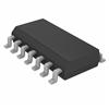
Pinout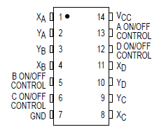 Specifications
|
Symbol |
Parameter |
Value |
Unit |
|
VCC |
Positive DC Supply Voltage (Referenced to GND) |
0.5 to +14.0 |
V |
|
VIS |
Analog Input Voltage (Referenced to GND) |
0.5 to VCC +0.5 |
V |
|
Iin |
Digital Input Voltage (Referenced to GND) |
0.5 to VCC +0.5 |
V |
|
I |
DC Current Into or Out of Any Pin |
± 25 |
mA |
|
PD |
Power Dissipation in Still Air, Plastic or Ceramic DIP†
SOIC Package†
TSSOP Package† |
750
500
450
|
mW |
|
Tstg |
Storage Temperature |
65 to + 150 |
|
|
TL |
Lead Temperature, 1 mm from Case for 10 Seconds
(Plastic DIP, SOIC or TSSOP Package)
(Ceramic DIP)
|
260
300 |
|
* Maximum Ratings are those values beyond which damage to the device may occur. Functional operation should
be restricted to the Recommended Operating Conditions.
†Derating - Plastic DIP: 10 mW/ from 65° to 125
Ceramic DIP: 10 mW/ from 100° to 125
SOIC Package: 7 mW/ from 65° to 125
TSSOP Package: 6.1 mW/ from 65° to 125
For high frequency or heavy load considerations, see Chapter 2 of the Motorola HighSpeed CMOS Data Book (DL129/D).
This device contains protection circuitry to guard against damage due to high static voltages or electric fields. However, precautions must be taken to avoid applications of any voltage higher than maximum rated voltages to this highimpedance circuit. For proper operation, Vin and Vout should be constrained to the range GND (Vin or Vout) VCC.
Unused inputs must always be tied to an appropriate logic voltage level (e.g., either GND or VCC). Unused outputs must be left open. I/O pins must be connected to a properly terminated line or bus.DescriptionThe MC54/74HC4066A utilizes silicongate CMOS technology to achieve fast propagation delays, low ON resistances, and low OFF channel leakage current. This bilateral switch/multiplexer/demultiplexer controls analog and digital voltages that may vary across the full powersupply range (from VCC to GND).
The HC4066A is identical in pinout to the metalgate CMOS MC14016 and MC14066. Each device has four independent switches. The device has been designed so that the ON resistances (RON) are much more linear over input voltage than RON of metalgate CMOS analog switches.
The ON/OFF control inputs are compatible with standard CMOS outputs; with pullup resistors, they are compatible with LSTTL outputs. For analog switches with voltagelevel translators, see the HC4316A.

 MC74HC4066A Data Sheet