SeekIC No. : 004417413
Detail
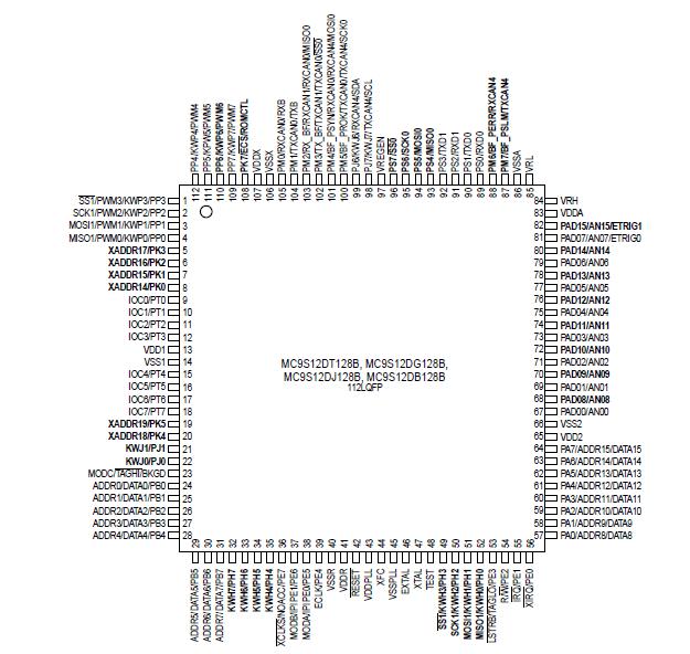
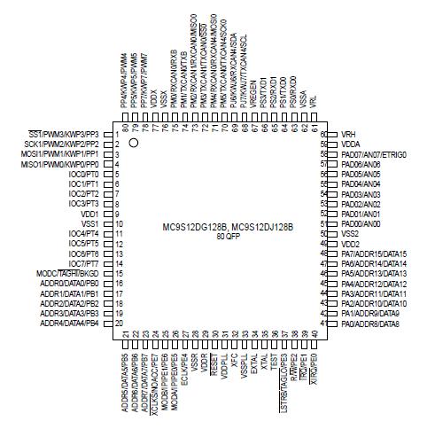
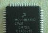
MC9S12DG128B: Features: • HCS12 Core 16-bit HCS12 CPUi. Upward compatible with M68HC11 instruction setii. Interrupt stacking and programmer's model identical to M68HC11iii.20-bit ALUiv. Instruction queuev. ...
 MC9S12DG128B Data Sheet
floor Price/Ceiling Price
- Part Number:
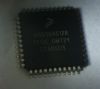
- MC9S12DG128B
- Supply Ability:
- 5000
Price Break
- Qty
- 1~5000
- Unit Price
- Negotiable
- Processing time
- 15 Days
SeekIC Buyer Protection PLUS - newly updated for 2013!
- Escrow Protection.
- Guaranteed refunds.
- Secure payments.
- Learn more >>
Month Sales
268 Transactions
Payment Methods
All payment methods are secure and covered by SeekIC Buyer Protection PLUS.
Notice: When you place an order, your payment is made to SeekIC and not to your seller. SeekIC only pays the seller after confirming you have received your order. We will also never share your payment details with your seller.