MCF5213EC

Features: • Version 2 ColdFire variable-length RISC processor core- Static operation- 32-bit address and data paths on-chip- Up to 80 MHz processor core frequency- Sixteen general-purpose, 32-bit data and address registers- Implements ColdFire ISA_A with extensions to support the user stack ...

product image

MCF5213EC Picture
SeekIC No. : 004417534 Detail

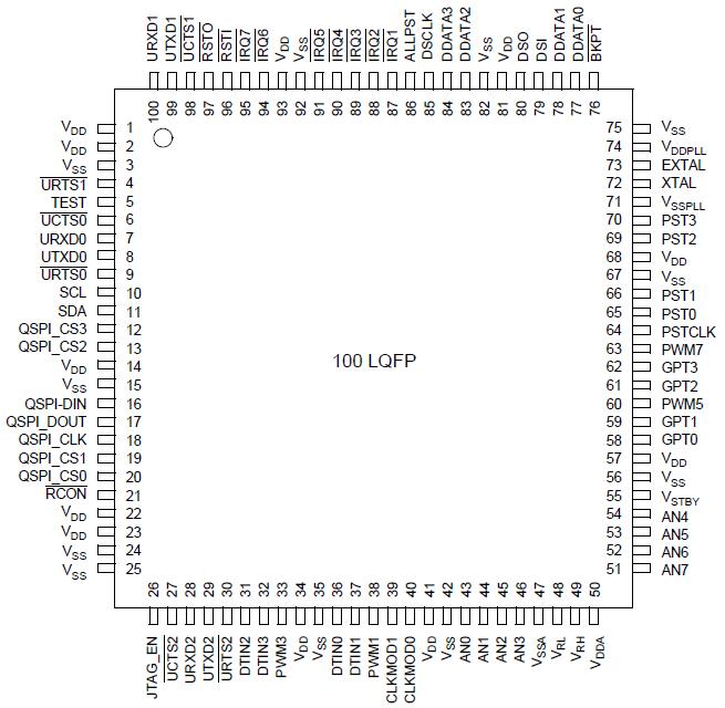
MCF5213EC: Features: • Version 2 ColdFire variable-length RISC processor core- Static operation- 32-bit address and data paths on-chip- Up to 80 MHz processor core frequency- Sixteen general-purpose, 32-...

floor Price/Ceiling Price

Part Number:
MCF5213EC
Supply Ability:
5000

Price Break

  • Qty
  • 1~5000
  • Unit Price
  • Negotiable
  • Processing time
  • 15 Days
Total Cost: $ 0.00

SeekIC Buyer Protection PLUS - newly updated for 2013!

  • Escrow Protection.
  • Guaranteed refunds.
  • Secure payments.
  • Learn more >>

Month Sales

268 Transactions

Rating

evaluate  (4.8 stars)

Upload time: 2024/4/27

Payment Methods

All payment methods are secure and covered by SeekIC Buyer Protection PLUS.

Notice: When you place an order, your payment is made to SeekIC and not to your seller. SeekIC only pays the seller after confirming you have received your order. We will also never share your payment details with your seller.
Product Details

Description


Features:

• Version 2 ColdFire variable-length RISC processor core
- Static operation
- 32-bit address and data paths on-chip
- Up to 80 MHz processor core frequency
- Sixteen general-purpose, 32-bit data and address registers
- Implements ColdFire ISA_A with extensions to support the user stack pointer register, and four new instructions for improved bit processing
- Multiply-Accumulate (MAC) unit with 32-bit accumulator to support 16 * 16 32 or 32 * 32 32 operations
- Illegal instruction decode that allows for 68K emulation support
• System debug support
- Real time trace for determining dynamic execution path
- Background debug mode (BDM) for in-circuit debugging
- Real time debug support, with six hardware breakpoints (4 PC, 1 address and 1 data) that can be configured into a 1- or 2-level trigger
• On-chip memories
- 32-Kbyte dual-ported SRAM on CPU internal bus, supporting core and DMA access with standby power supply support
- 256 Kbytes of interleaved Flash memory supporting 2-1-1-1 accesses
• Power management
- Fully static operation with processor sleep and whole chip stop modes
- Very rapid response to interrupts from the low-power sleep mode (wake-up feature)
- Clock enable/disable for each peripheral when not used
• FlexCAN 2.0B Module
- Based on and includes all existing features of the Freescale TouCAN module
- Full implementation of the CAN protocol specification version 2.0B
    Standard Data and Remote Frames (up to 109 bits long)
    Extended Data and Remote Frames (up to 127 bits long)
    0-8 bytes data length
    Programmable bit rate up to 1 Mbit/sec
- Flexible Message Buffers (MBs), totalling up to 16 message buffers of 08 byte data length each, configurable as Rx or Tx, all supporting standard and extended messages
- Unused MB space can be used as general purpose RAM space
- Listen only mode capability
- Content-related addressing
- No read/write semaphores
- Three programmable mask registers: global for MBs 0-13, special for MB14, and special for MB15
- Programmable transmit-first scheme: lowest ID or lowest buffer number
- "Time stamp" based on 16-bit free-running timer
- Global network time, synchronized by a specific message
- Maskable interrupts
• Three Universal Asynchronous/synchronous Receiver Transmitters (UARTs)
- 16-bit divider for clock generation
- Interrupt control logic with maskable interrupts
- DMA support
- Data formats can be 5, 6, 7 or 8 bits with even, odd or no parity
- Up to 2 stop bits in 1/16 increments
- Error-detection capabilities
- Modem support includes request-to-send (RTS) and clear-to-send (CTS) lines for two UARTs
- Transmit and receive FIFO buffers
• I2C Module
- Interchip bus interface for EEPROMs, LCD controllers, A/D converters, and keypads
- Fully compatible with industry-standard I2C bus
- Master and slave modes support multiple masters
- Automatic interrupt generation with programmable level
• Queued Serial Peripheral Interface (QSPI)
- Full-duplex, three-wire synchronous transfers
- Up to four chip selects available
- Master mode operation only
- Programmable bit rates up to half the CPU clock frequency
- Up to 16 pre-programmed transfers
• Fast Analog-to-Digital Converter (ADC)
- Eight analog input channels
- 12-bit resolution ± 2.5 counts accuracy
- Minimum 2.25 s conversion time
- Simultaneous sampling of two channels for motor control applications
- Single-scan or continuous operation
- Optional interrupts on conversion complete, zero crossing (sign change), or under/over low/high limit
- Unused analog channels can be used as digital I/O
• Four 32-bit DMA Timers
- 12.5-ns resolution at 80 MHz
- Programmable sources for clock input, including an external clock option
- Programmable prescaler
- Input capture capability with programmable trigger edge on input pin
- Output compare with programmable mode for the output pin
- Free run and restart modes
- Maskable interrupts on input capture or output compare
- DMA trigger capability on input capture or output compare
• Four-channel General Purpose Timers
- 16-bit architecture
- Programmable prescaler
- Output pulse widths variable from microseconds to seconds
- Single 16-bit input pulse accumulator
- Toggle-on-overflow feature for pulse-width modulator (PWM) generation
- One dual-mode pulse accumulation channel
• Pulse-Width Modulation Timer
- Operates as eight channels with 8-bit resolution or four channels with 16-bit resolution
- Programmable period and duty cycle
- Programmable enable/disable for each channel
- Software selectable polarity for each channel
- Period and duty cycle are double buffered. Change takes effect when the end of the current period is reached (PWM counter reaches zero) or when the channel is disabled.
- Programmable center or left aligned outputs on individual channels
- Four clock sources (A, B, SA, and SB) provide for a wide range of frequencies
- Emergency shutdown
• Two Periodic Interrupt Timers (PITs)
- 16-bit counter
- Selectable as free running or count down
• Software Watchdog Timer
- 16-bit counter
- Low power mode support
• Clock Generation Features
- 1 to 16 MHz crystal, 8 MHz on-chip relaxation oscillator, or external oscillator reference options
- Relaxation oscillator NVM-trimmed to 2% accuracy
- 2 to 10 MHz reference frequency for normal PLL mode
- System can be clocked from PLL or directly from crystal oscillator or relaxation oscillator
- Low power modes supported
- 2n (n 0 15) low-power divider for extremely low frequency operation
• Interrupt Controller
- Support for up to 56 interrupt sources organized as follows:
    49 fully-programmable interrupt sources
    7 fixed-level interrupt sources
- Seven external interrupt signals
- Unique vector number for each interrupt source
- Ability to mask any individual interrupt source or all interrupt sources (global mask-all)
- Support for hardware and software interrupt acknowledge (IACK) cycles
- Combinatorial path to provide wake-up from low power modes
• DMA Controller
- Four fully programmable channels
- Dual-address transfer support with 8-, 16-, and 32-bit data capability, along with support for 16-byte (4 x 32-bit) burst transfers
- Source/destination address pointers that can increment or remain constant
- 24-bit byte transfer counter per channel
- Auto-alignment transfers supported for efficient block movement
- Bursting and cycle steal support
- Software-programmable DMA requesters for the UARTs (3) and 32-bit timers (4)
• Reset
- Separate reset in and reset out signals
- Seven sources of reset:
    Power-on reset (POR)
    External
    Software
    Watchdog (resets the CPU without affecting the peripheral modules)
    Loss of clock
    Loss of lock
    Low-voltage detection (LVD)
- Status flag indication of source of last reset
• Chip Integration Module (CIM)
- System configuration during reset
- Selects one of six clock modes
- Configures output pad drive strength
- Unique part identification number and part revision number
• General Purpose I/O interface
- Up to 56 bits of general purpose I/O
- Bit manipulation supported via set/clear functions
- Programmable drive strengths of 2mA or 10mA per pin
- Unused peripheral pins may be used as extra GPIO
• JTAG support for system level board testing


Pinout

  Connection Diagram


Specifications

Rating
Symbol
Value
Unit
Supply Voltage
VDD
0.3 to +4.0
V
Clock Synthesizer Supply Voltage
VDDPLL
0.3 to +4.0
V
RAM Memory Standby Supply Voltage
VSTBY
0.3 to +4.0
V
Digital Input Voltage 3
VIN
0.3 to +4.0
V
EXTAL pin voltage
VEXTAL
0 to 3.3
V
XTAL pin voltage
VXTAL
0 to 3.3
V
Instantaneous Maximum Current
Single pin limit (applies to all pins) 4, 5
IDD
25
mA
Operating Temperature Range (Packaged)
TA
(TL - TH)
40 to 85
°C
Storage Temperature Range
Tstg
65 to 150
°C


Customers Who Bought This Item Also Bought

Margin,quality,low-cost products with low minimum orders. Secure your online payments with SeekIC Buyer Protection.
View more