MD1811

Features: · 6ns rise and fall time· 2 A peak output source/sink current· 1.2V to 5V input CMOS compatible· 5V to 12V total supply voltage· Smart Logic threshold· Low jitter design· Quad matched channels· Drives two N and two P Channel MOSFETs· Outputs can swing below ground· Low inductance quad fl...

product image

MD1811 Picture
SeekIC No. : 004418832 Detail

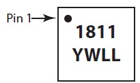
MD1811: Features: · 6ns rise and fall time· 2 A peak output source/sink current· 1.2V to 5V input CMOS compatible· 5V to 12V total supply voltage· Smart Logic threshold· Low jitter design· Quad matched chan...

floor Price/Ceiling Price

Part Number:
MD1811
Supply Ability:
5000

Price Break

  • Qty
  • 1~5000
  • Unit Price
  • Negotiable
  • Processing time
  • 15 Days
Total Cost: $ 0.00

SeekIC Buyer Protection PLUS - newly updated for 2013!

  • Escrow Protection.
  • Guaranteed refunds.
  • Secure payments.
  • Learn more >>

Month Sales

268 Transactions

Rating

evaluate  (4.8 stars)

Upload time: 2024/4/28

Payment Methods

All payment methods are secure and covered by SeekIC Buyer Protection PLUS.

Notice: When you place an order, your payment is made to SeekIC and not to your seller. SeekIC only pays the seller after confirming you have received your order. We will also never share your payment details with your seller.
Product Details

Description


Features:

· 6ns rise and fall time
· 2 A peak output source/sink current
· 1.2V to 5V input CMOS compatible
· 5V to 12V total supply voltage
· Smart Logic threshold
· Low jitter design
· Quad matched channels
· Drives two N and two P Channel MOSFETs
· Outputs can swing below ground
· Low inductance quad fl at no-lead package
· High-performance thermally-enhanced


Application

· Medical ultrasound imaging
· Piezoelectric transducer drivers
· Nondestructive evaluation
· PIN diode driver
· Clock driver/buffer
· High speed level translator


Pinout

  Connection Diagram


Specifications

VDD-VSS, Logic Supply Voltage
-0.5V to +13.5V
VH, Output High Supply Voltage
VL-0.5V to VDD+0.5V
VL, Output Low Supply Voltage
VSS-0.5V to VH+0.5V
Vss, Low Side Supply Voltage
-7V to +0.5V
Logic Input Levels
VSS-0.5V to VSS+7V
Maximum Junction Temperature
+125°C
Storage Temperature
-65°C to 150°C
Soldering Temperature
235°C
Package Power Dissipation
2.2W

*Absolute Maximum Ratings are those values beyond which damage to the device may occur. Functional operation under these conditions is not implied. Continuous operation of the device at the absolute rating level may affect device reliability. All voltages are referenced to device ground.


Description

The Supertex MD1811 is a high speed, quad MOSFET driver designed to drive high voltage P/N-channel MOSFETs for medical ultrasound applications and other applications requiring a high output current for a capacitive load. The high-speed input stage of the MD1811 can operate from a 1.2 to 5.0 volt logic interface with an optimum operating input signal range of 1.8 to 3.3 volts. An adaptive threshold circuit is used to set the level translator switch threshold to the average of the input logic 0 and logic 1 levels. The input logic levels may be ground referenced, even though the driver is putting out bipolar signals. The level translator uses a proprietary circuit, which provides DC coupling together with high-speed operation.

The output stage of the MD1811 has separate power connections enabling the output signal L and H levels to be chosen independently from the supply voltages used for the majority of the circuit. As an example, the input logic levels may be 0 and 1.8 volts, the control logic may be powered by +5 and 5 volts, and the output L and H levels may be varied anywhere over the range of 5 to +5 volts. The output stage is capable of peak currents of up to ±2 amps, depending on the supply voltages used and load capacitance present. The OE pin serves a dual purpose. First, its logic H level is used to compute the threshold voltage level for the channel input level translators. Secondly, when OE is low, the outputs are disabled, with the A & C output high and the B & D output low. This assists in properly pre-charging the AC coupling capacitors that may be used in series in the gate drive circuit of an external PMOS and NMOS transistor pair.


Customers Who Bought This Item Also Bought

Margin,quality,low-cost products with low minimum orders. Secure your online payments with SeekIC Buyer Protection.
Crystals and Oscillators
Computers, Office - Components, Accessories
Cable Assemblies
Cables, Wires - Management
Fans, Thermal Management
View more