| Pin Number |
Pin Name |
Pin Function |
|
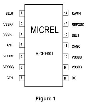
1 |
SEL0 |
Programs desired Demodulator Filter Bandwidth. This pin in internally pulled-up to VDD. See Table 1. |
|
2/3 |
VSSRF |
This pin is the ground return for the RF section of the IC. The bypass capacitor connected from VDDRF to
VSSRF should have the shortest possible lead length. For best performance, connect VSSRF to VSSBB at the
power supply only (i.e., keep VSSBB currents from flowing through VSSRF return path). |
|
4 |
ANT |
This is the receive RF input, internally ac-coupled. Connect this pin to the receive antenna. Input
impedance is high (FET gate) with approximately 2pF of shunt (parasitic) capacitance. For applications
located in high ambient noise environments, a fixed value band-pass network may be connected between
the ANT pin and VSSRF to provide additional receive selectivity and input overload protection. (See
"Application Note 22, MICRF001 Theory of Operation".) |
|
5 |
VDDRF |
This pin is the positive supply input for the RF section of the IC. VDDBB and VDDRF should be connected
directly at the IC pins. Connect a low ESL, low ESR decoupling capacitor from this pin to VSSRF, as short
as possible. |
|
6 |
VDDBB |
This pin is the positive supply input for the baseband section of the IC. VDDBB and VDDRF should be
connected directly at the IC pins. |
|
7 |
CTH |
This capacitor extracts the (DC) average value from the demodulated waveform, which becomes the
reference for the internal data slicing comparator. Treat this as a low-pass RC filter with source impedance
described in Table 1 . (See "Application Note 22, MICRF001 Theory of Operation", section 6.4). A
standard ± 20% X7R ceramic capacitor is generally sufficient. |
|
8 |
DO |
Output data pin. CMOS level compatible. |
|
9/10 |
VSSBB |
This is the ground return for the baseband section of the IC. The bypass and output capacitors connected
to VSSBB should have the shortest possible lead lengths. For best performance, connect VSSRF to
VSSBB at the power supply only (i.e., keep VSSBB currents from flowing through VSSRF return path). |
|
8 |
N/C |
Unused Pin |
|
9 |
VSSBB |
This is the ground return for the baseband section of the IC. The bypass and output capacitors connected to
VSSBB should have the shortest possible lead lengths. For best performance, connect VSSRF to VSSBB at
the power supply only (i.e., keep VSSBB currents from flowing through VSSRF return path). |
|
11 |
CAGC |
The output data signal. CMOS level compatible. |
|
12 |
SEL1 |
Programs desired Demodulator Filter Bandwidth. This pin in internally pulled-up to VDD. See Table 1. |
|
13 |
REFOSC |
This is the timing reference for on-chip tuning and alignment. Either connect a ceramic resonator between
this pin and VSSBB, or drive the input with an AC coupled 0.5Vpp input clock. Use ceramic resonators
without integral capacitors. See "Application Note 22, MICRF001 Theory of Operation" for details on
frequency selection and accuracy. |
|
14 |
SWEN |
This logic pin controls the operating mode of the MICRF001. When SWEN = HIGH, the MICRF001 is in
SWP mode. This is the normal (default) mode of the device. When SWEN = LOW, the device operates as
a conventional single-conversion superheterodyne receiver. (See "Application Note 22, MICRF001 Theory
of Operation" for details.) This pin is internally pulled-up to VDD. |

 MICRF001 Data Sheet