Features: • Very Low Total Harmonic Distortion• Low Glitch Energy• Fast Settling Time• Four Quadrant Multiplication• On-Chip Latches for Both DACs• 4.5 V to 5.5 V Operation• Low Power Consumption• TTL/5V CMOS Compatible• Latch-Up Free• 15...
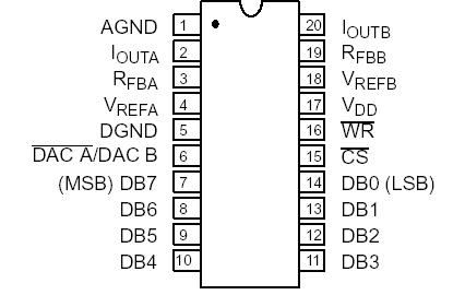
MP7529B: Features: • Very Low Total Harmonic Distortion• Low Glitch Energy• Fast Settling Time• Four Quadrant Multiplication• On-Chip Latches for Both DACs• 4.5 V to 5.5 V...
SeekIC Buyer Protection PLUS - newly updated for 2013!
268 Transactions
All payment methods are secure and covered by SeekIC Buyer Protection PLUS.

| VDD to AGND VDD to DGND Digital Input Voltage to DGND Any IOUT1, IOUT2 to AGND Any VREF to AGND AGND to DGND (Functionality Guaranteed ±0.5 V) |
-0 to +7 V -0.5 to +7 V GND -0.5 to VDD +0.5 V GND -0.5 to VDD +0.5 V ±25 V ±1 V |
| Any VRFB to AGND Storage Temperature Lead Temperature (Soldering, 10 seconds) Package Power Dissipation Rating to 75°C CDIP, PDIP, PQFP Derates above 75°C |
±25 V -65°C to +150°C +300°C 800mW 12mW/°C |
NOTES:
1 Stresses above those listed under "Absolute Maximum Ratings" may cause permanent damage to the device. This is a stress rating only and functional operation at or above this specification is not implied. Exposure to maximum rating conditions for extended periods may affect device reliability.
2 Any input pin which can see a value outside the absolute maximum ratings should be protected by Schottky diode clamps (HP5082-2835) from input pin to the supplies. All inputs have protection diodes which will protect the device from short transients outside the supplies of less than 100mA for less than 100ms.
3 GND refers to AGND and DGND.
The MP7529B is a dual 8-bit Digital-to-Analog Converter featuring excellent DAC to DAC matching, tracking and specifically optimized for applications requiring low total harmonic distortion. It is manufactured using advanced thin film resistors on a double metal CMOS process. The MP7529B incorporates a unique bit decoding technique yielding lower glitch energy, higher speed and excellent accuracy over temperature and time.
Data of MP7529B is transferred to either of the two D/A Converter latches via a common 8-bit TTL/5 V CMOS compatible input port. The control input DAC A/DAC B determines which D/A is to be loaded.
The MP7529B operates from a 4.5 V to 5.5 V power supply, and is TTL-compatible over this range. Power dissipation is only 10 mW. Both DACs offer excellent four quadrant multiplication characteristics, and include separate reference inputs and feedback resistors. An improved latch-up resistant design of MP7529B eliminates the need for external protective Schottky diodes in most applications.