MP8775

Features: · 8-Bit Resolution· 20 MHz Sampling Rate· DNL = +1/2 LSB, INL = +1 LSB (typ)· Internal S/H Function· Single Supply: 5 V· VIN DC Range: 0 V to VDD· VREF DC Range: 1 V to VDD· Low Power: 85 mW typ. (excluding reference)· Latch-Up Free· ESD Protection: 2000 V MinimumApplication` Digital Col...

product image

MP8775 Picture
SeekIC No. : 004425959 Detail

MP8775: Features: · 8-Bit Resolution· 20 MHz Sampling Rate· DNL = +1/2 LSB, INL = +1 LSB (typ)· Internal S/H Function· Single Supply: 5 V· VIN DC Range: 0 V to VDD· VREF DC Range: 1 V to VDD· Low Power: 85 ...

floor Price/Ceiling Price

Part Number:
MP8775
Supply Ability:
5000

Price Break

  • Qty
  • 1~5000
  • Unit Price
  • Negotiable
  • Processing time
  • 15 Days
Total Cost: $ 0.00

SeekIC Buyer Protection PLUS - newly updated for 2013!

  • Escrow Protection.
  • Guaranteed refunds.
  • Secure payments.
  • Learn more >>

Month Sales

268 Transactions

Rating

evaluate  (4.8 stars)

Upload time: 2024/4/27

Payment Methods

All payment methods are secure and covered by SeekIC Buyer Protection PLUS.

Notice: When you place an order, your payment is made to SeekIC and not to your seller. SeekIC only pays the seller after confirming you have received your order. We will also never share your payment details with your seller.
Product Details

Description


Features:

· 8-Bit Resolution
· 20 MHz Sampling Rate
· DNL = +1/2 LSB, INL = +1 LSB (typ)
· Internal S/H Function
· Single Supply: 5 V
· VIN DC Range: 0 V to VDD
· VREF DC Range: 1 V to VDD
· Low Power: 85 mW typ. (excluding reference)
· Latch-Up Free
· ESD Protection: 2000 V Minimum


Application

` Digital Color Copiers
` Cellular Telephones
` CCD's Based Systems
` Hardware Scanners
` Video Capture Boards


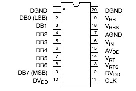
Pinout

  Connection Diagram


Specifications

VDD to GND  . . . . . . . . . . . . . . . . . . . . . . .  . . . . . . . . . . . . . . .7 V
VRT & VRB . . . . . . . . . . . . . . . . . . . . . . .  VDD +0.5 to GND --0.5 V
VIN  . . . . . . . . . . . . . . . . . . . . . .. .  . . . . .VDD +0.5 to GND --0.5 V
All Inputs  . . . . . . . . . . . . . . . . . . ..  . . . .VDD +0.5 to GND --0.5 V
All Outputs  . . . . . . . . . . . . . . . . .. .  . . . .VDD +0.5 to GND --0.5 V
Storage Temperature . . . . . . . . . . . . . . . . .  . . . . --65 to +150°C
Lead Temperature (Soldering 10 seconds)  . . . . . .. . . . . .+300°C
Package Power Dissipation Rating @ 75°C
SOIC, SSOP, PDIP . . . . . . . . . . . . . . . . . . . . . . . . . . . .  . .700 mW
Derates above 75°C . . . . . . . . . . . . . . . . . . . . . . . . . . . 9 mW/°C

Notes:
1 Stresses above those listed under "Absolute Maximum Ratings" may cause permanent damage to the device. This is a stress rating only and functional operation at or above this specification is not implied. Exposure to maximum rating conditions for extended periods may affect device reliability.
2 Any input pin which can see a value outside the absolute maximum ratings should be protected by Schottky diode clamps (HP5082-2835) from input pin to the supplies. All inputs have protection diodes which will protect the device from short transients outside the supplies of less than 100mA for less than 100ms.
3 VDD refers to AVDD and DVDD. GND refers to AGND and DGND.


Description

The MP8775 is an 8-bit Analog-to-Digital Converter in a small 20 pin SOIC package. Designed using an advanced 5 V CMOS process, this part offers excellent performance, low power consumption and latch-up free operation.

This device uses a two-step flash architecture tomaintain low power consumption at high conversion rates. The input circuitry of the MP8775 includes an on-chip S/H function and allows the user to digitize analog input signals between GND and VDD. Careful design and chip layout have achieved a low analog input capacitance. This reduces "kickback" and eases the requirements of the buffer/amplifier used to drive the MP8775.

The designer of MP8775 can choose the internally generated reference voltages by connecting VRB to VRBS and VRT to VRTS, or provide external reference voltages to the VRB and VRT pins. The internal reference generates 0.6 V at VRB and 2.6 V at VRT. Providing external reference voltages allows easy interface to any input signal range between GND and VDD. MP8775 also allows the system to adjust these voltages to cancel zero scale and full scale errors, or to change the input range as needed.

The MP8775 operates from a single +5 V supply. Power consumption is 85 mW at Fs = 20 MHz.

MP8775 is specified for operation over the commercial / industrial (--40 to +85°C) temperature range, the MP8775 is available in Surface Mount (SOIC), Shrunk Small Outline (SSOP) and Plastic dual-in-line (PDIP) packages.


Customers Who Bought This Item Also Bought

Margin,quality,low-cost products with low minimum orders. Secure your online payments with SeekIC Buyer Protection.
Integrated Circuits (ICs)
Programmers, Development Systems
Static Control, ESD, Clean Room Products
Prototyping Products
DE1
Industrial Controls, Meters
View more