Specifications
| Rating |
Symbol |
Value |
Unit |
| DrainSource Voltage |
VDSS |
65 |
Vdc |
| GateSource Voltage |
VGS |
0.5, +15 |
Vdc |
Total Device Dissipation @ TC = 25°C
Derate above 25°C |
PD |
261
1.49 |
Watts
W/°C |
| Storage Temperature Range |
Tstg |
65 to +200 |
°C |
| Operating Junction Temperature |
TJ |
200 |
°C |
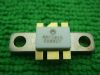
DescriptionThe MRF5S19090LSR3 has eleven features.(1)typical 2 -carrier N-CDMA performance for VDD = 28 Volts, IDQ =1200 mA, pout = 26 watts avg., full frequency band, IS-95 CDMA (Pilot,Sync, Paging, Traffic Codes 8 Through 13) channel bandwidth =1.2288 MHz. peak/Avg. = 9.8 dB @ 0.01% probability on CCDF.(2)internally matched, controlled Q, for ease of Use.(3)high gain, high efficiency and high linearity.(4)integrated ESD protection.(5)designed for maximum gain and insertion phase flatness.(6)capable of handling 10:1 VSWR, @ 28 Vdc, 1960 MHz,90 watts CW output power.(7)excellent thermal stability.(8)characterized with series equivalent largesignal impedance parameters.(9)qualified up to a maximum of 32 VDD operation.(10)available in tape and reel. R3 suffix = 250 units per 56 mm, 13 inch reel.(11)low gold plating thickness on leads. L suffix indicates 40 Nominal.
MRF5S19090LSR3 Information in this document is provided solely to enable system and software implementers to use Freescale Semiconductor products. There are no express or implied copyright licenses granted hereunder to design or fabricate any integrated circuits or integrated circuits based on the information in this document.
MRF5S19090LSR3 Freescale Semiconductor reserves the right to make changes without further notice to any products herein. Freescale Semiconductor makes no warranty, representation or guarantee regarding the suitability of its products for any particular purpose, nor does Freescale Semiconductor assume any liability arising out of the application or use of any product or circuit, and specifically disclaims any and all liability, including without limitation consequential or incidental damages. "Typical" parameters that may be provided in Freescale Semiconductor data sheets and/or specifications can and do vary in different applications and actual performance may vary over time. All operating parameters, including "Typicals", must be validated for each customer application by customer's technical experts. Freescale Semiconductor does not convey any license under its patent rights nor the rights of others. Freescale Semiconductor products are not designed, intended, or authorized for use as components in systems intended for surgical implant into the body, or other applications intended to support or sustain life,or for any other application in which the failure of the Freescale Semiconductor product could create a situation where personal injury or death may occur. Should Buyer purchase or use Freescale Semiconductor products for any such unintended or unauthorized application, Buyer shall indemnify and hold Freescale Semiconductor and its officers, employees, subsidiaries, affiliates, and distributors harmless against all claims, costs, damages, and expenses, and reasonable attorney fees arising out of,directly or indirectly, any claim of personal injury or death associated with such unintended or unauthorized use, even if such claim alleges that Freescale Semiconductor was negligent regarding the design or manufacture of the part.

 MRF5S19090LSR3 Data Sheet