MS81V04160A

Features: • 262,214 words × 8 bits × 2• Fast FIFO (First-In First-Out) Operation: 25 ns cycle time• Self refresh (No refresh control is required)• High speed asynchronous serial access Read/Write Cycle Time 20 ns/25 ns Access Time 18 ns/23 ns• Variable length delay bi...

product image

MS81V04160A Picture
SeekIC No. : 004427432 Detail

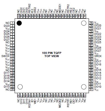
MS81V04160A: Features: • 262,214 words × 8 bits × 2• Fast FIFO (First-In First-Out) Operation: 25 ns cycle time• Self refresh (No refresh control is required)• High speed asynchronous ser...

floor Price/Ceiling Price

Part Number:
MS81V04160A
Supply Ability:
5000

Price Break

  • Qty
  • 1~5000
  • Unit Price
  • Negotiable
  • Processing time
  • 15 Days
Total Cost: $ 0.00

SeekIC Buyer Protection PLUS - newly updated for 2013!

  • Escrow Protection.
  • Guaranteed refunds.
  • Secure payments.
  • Learn more >>

Month Sales

268 Transactions

Rating

evaluate  (4.8 stars)

Upload time: 2024/4/27

Payment Methods

All payment methods are secure and covered by SeekIC Buyer Protection PLUS.

Notice: When you place an order, your payment is made to SeekIC and not to your seller. SeekIC only pays the seller after confirming you have received your order. We will also never share your payment details with your seller.
Product Details

Description


Features:

• 262,214 words × 8 bits × 2
• Fast FIFO (First-In First-Out) Operation: 25 ns cycle time
• Self refresh (No refresh control is required)
• High speed asynchronous serial access Read/Write Cycle Time 20 ns/25 ns Access Time 18 ns/23 ns
• Variable length delay bit (150 to 262214)
• Write mask function (Output enable control)
• Cascading capability by mode setting
• Single power supply: 3.3 V ± 0.3V
• Package: 100-Pin plastic TQFP (TQFP 100-P-1414-0.50-k) (Product: MS81V04160A-xxTB)


Pinout

  Connection Diagram


Specifications

Parameter
Symbol
Condition
Rating
Unit
Input Output Voltage
VT
at Ta = 25, VSS
1.0 to +5.5
V
Output Current
IOS
Ta = 25
50
mA
Power Dissipation
PD
Ta = 25
1
W
Operating Temperature
TOPR
-
0 to 70
Storage Temperature
TSTG
-
-55 to +150


Description

The MS81V04160A is a single-chip 4Mb FIFO functionally composed of two OKI 2Mb FIFO (First-In First-Out) memories which were designed for 262,214 x 8-bit high-speed asynchronous read/write operation.

The read clocks and the write clocks of each of the 2Mb FIFO memories are connected in common. The MS81V04160A, functionally compatible with Oki's 2Mb FIFO memory (MSM51V8222A), can be used as a x16 configuration FIFO.

The MS81V04160A is a field memory for wide or low end use in general commodity TVs and VTRs exclusively and is not designed for high end use in professional graphics systems, which require long term picture storage, data storage, medical use and other storage systems.

The MS81V04160A provides independent control clocks to support asynchronous read and write operations.
Different clock rates are also supported, which allow alternate data rates between write and read data streams. It provides high speed FIFO (First-in First-out) operation without external refreshing: MS81V04160A refreshes its DRAM storage cells automatically, so that it appears fully static to the users.

More about MS81V04160A, fully static type memory cells and decoders for serial access enable the refresh free serial access operation, so that serial read and/or write control clock can be halted high or low for any duration as long as the power is on. Internal conflicts of memory access and refreshing operations are prevented by special arbitration logic.

The MS81V04160A's function is simple, and similar to a digital delay device whose delay-bit- length is easily set by reset timing. The delay length and the number of read delay clocks between write and read, is determined by externally controlled write and read reset timings.

MS81V04160A's Additional SRAM serial registers, or line buffers for the initial access of 71 x 16-bit enable high speed first-bit-access with no clock delay just after the write or read reset timings.

Additionally, the MS81V04160A has a write mask function or input enable function (IE), and read- data skipping function or output enable function (OE). The differences between write enable (WE) and input enable (IE), and  between read enable (RE) and output enable (OE) are that WE and RE can stop serial write/read address increments, but IE and OE cannot stop the increment, when write/read clocking is continuously applied to MS81V04160A. The input enable (IE) function allows the user to write into selected locations of the memory only, leaving the rest of the memory contents unchanged. This facilitates data processing to display a "picture in picture" on a TV screen.


Customers Who Bought This Item Also Bought

Margin,quality,low-cost products with low minimum orders. Secure your online payments with SeekIC Buyer Protection.
Batteries, Chargers, Holders
Power Supplies - External/Internal (Off-Board)
Prototyping Products
DE1
Circuit Protection
Transformers
View more