Pinout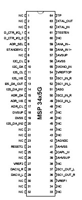 Specifications
|
Symbol |
Parameter |
Pin Name |
Min. |
Max. |
Unit |
|
TA |
Ambient Operating Temperature |
|
0 |
70 |
|
|
TS |
Storage Temperature |
|
-40 |
125 |
|
|
VSUP1 |
First Supply Voltage |
AHVSUP |
-0.3
|
9.0 |
V |
|
VSUP2 |
Second Supply Voltage |
DVSUP |
-0.3 |
6.0 |
V |
|
VSUP3 |
Third Supply Voltage |
AVSUP |
-0.3 |
6.0 |
V |
|
dVSUP23 |
Voltage between AVSUP
and DVSUP |
AVSUP,
DVSUP |
-0.5 |
0.5 |
V |
|
PTOT |
Package Power Dissipation
PSDIP64
PSDIP52
PQFP80
PLQFP64
PMQFP44 |
AHVSUP,
DVSUP,
AVSUP |
|
1300
1200
1000
960
960 |
mW
mW
mW
mW
mW |
|
VIdig |
Input Voltage, all Digital Inputs |
|
-0.3
|
V +0.3SUP2 |
V |
|
IIdig |
Input Current, all Digital Pins |
|
-20
|
+20 |
mA1) |
|
VIana |
Input Voltage, all Analog Inputs |
SCn_IN_s,MONO_IN2) |
-0.3
|
V +0.3SUP1 |
V |
|
IIana |
Input Current, all Analog Inputs |
SCn_IN_s,MONO_IN2)
|
-5
|
+5 |
mA1) |
|
IOana |
Output Current, all SCART Outputs |
SC1_OUT_s 2)
|
3) 4)
, |
3) 4)
, |
|
|
IOana |
Output Current, all Analog Outputs
except SCART Outputs |
DACM_s 2) |
3) |
3) |
|
|
ICana |
Output Current, other pins
connected to capacitors |
CAPL_M, AGNDC |
3) |
3) |
|
1) positive value means current flowing into the circuit
2) "n" means "1" or "2", "s" means "L" or "R"
3) The Analog Outputs are short-circuit proof with respect to First Supply Voltage and Ground.
4) Total chip power dissipation must not exceed absolute maximum rating.
DescriptionPin numbers refer to the PQFP80 package
MSP34x5G features:
Pin 1, NC Pin not connected
Pin 2, I2C_CL I2 C Clock Input/Output (Fig. 418)Via this pin the I2C bus clock signal has to be supplied.
The signal can be pulled down by the MSP in case ofwait conditions.
Pin 3, I2C_DA I2C Data Input/Output (Fig. 418)Via this pin the I2C bus data is written to or read from the MSP.
Pin 4, I2S_CL I2S Clock Input/Output (Fig. 419)Clock line for the I2S bus. In master mode, this line isdriven by the MSP; in slave mode, an external I2Sclock has to be supplied.
Pin 5, I2S_WS I2S Word Strobe Input/Output (Fig. 419)wrd strobe line for the I2S bus. In master mode, thisline is driven by the MSP; in slave mode, an externalI2 S word strobe has to be supplied.
Pin 6, I2S_DA_OUT I2S Data Output (Fig. 423)Output of digital serial sound data of the MSP on theI2S bus.
Pin 7, I2S_DA_IN1 I2S Data Input 1 (Fig. 417)First input of digital serial sound data to the MSP viathe I2S bus.
Pin 8, ADR_DA ADR Bus Data Output (Fig. 423)Output of digital serial data to the DRP 3510A via theADR bus.
Pin 9, ADR_WS ADR Bus Word Strobe Output (Fig. 423)Word strobe output for the ADR bus.
Pin 10, ADR_CL ADR Bus Clock Output (Fig. 423)Clock line for the ADR bus.
Pins 11, 12, 13, DVSUP* Digital Supply Voltage Pwer supply for the digital circuitry of the MSP. Must e connected to a +5-V power supply.
Pins 14, 15, 16, DVSS* Digital Ground round connection for the digital circuitry of the MSP in 17, I2S_DA_IN2 I2S Data Input 2 (Fig. 417) econd input of digital serial sound data to the MSP ia the I S bus.
Pins 18, 19, 20, NC Pins not connected Pin 21, RESETQ Reset Input (Fig. 411) In the steady state, high level is required. A low level resets the MSP 34x0G.
Pins 22, 23, 24, 25, NC Pins not connected Pin 26, VREF2 Reference Ground 2 Reference analog ground. This pin must be connected separately to ground (AHVSS). VREF2 serves as a clean ground and should be used as the reference for analog connections to the loudspeaker and head-phone outputs.
Pins 27, 28, DACM_R/L Loudspeaker Outputs (Fig. 421) Output of the loudspeaker signal. A 1nF capacitor to AHVSS must be connected to these pins. The DC off-set on these pins depends on the selected loud-speaker volume.
Pins 29, 30, 31, 32, 33, 34, NC Pins not connected Pin 35, VREF1 Reference Ground 1 Reference analog ground. This pin must be connected separately to ground (AHVSS). VREF1 serves as a clean ground and should be used as the reference for analog connections to the SCART outputs.
Pins 36, 37, SC1_OUT_R/L SCART1 Outputs (Fig. 422) Output of the SCART1 signal. Connections to these pins must use a 100 ohm series resistor and are intended to be AC coupled.
Pin 38, NC Pin not connected Pin 39, AHVSUP* Analog Power Supply High Voltage Power is supplied via this pin for the analog circuitry of the MSP (except IF input). This pin must be connected to the +8V supply.
Pin 40, CAPLM Volume Capacitor Loudspeakers (Fig. 424) A 10F capacitor to AHVSUP must be connected to this pin. It serves as smoothing filter for loudspeaker volume changes in order to suppress audible plops.
The value of the capacitor can be lowered to 1F if faster response is required. The area encircled by the trace lines should be minimized, keep traces as short as possible. This input is sensitive for magnetic induc-tion.
Pins 41, 42, NC Pins not connected.
Pins 43, 44, AHVSS* Ground for Analog Power Sup-ply High Voltage Ground connection for the analog circuitry of the MSP (except IF input).
Pins 45, AGNDC Internal Analog Reference Voltage This pin serves as the internal ground connection for the analog circuitry (except IF input). It must be con-nected to the VREF pins with a 3.3 F and a 100 nF capacitor in parallel. This pins shows a DC level of typ-ically 3.73 V.

 MSP34x5G Data Sheet