MT28C3212P2FL

Features: • Flexible dual-bank architecture• Support for true concurrent operations with no latency: Read bank b during program bank a and vice versa Read bank b during erase bank a and vice versa• Organization: 2,048K x 16 (Flash) 128K x 16 (SRAM)• Basic configuration: Fla...

product image

MT28C3212P2FL Picture
SeekIC No. : 004429666 Detail

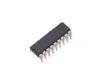
MT28C3212P2FL: Features: • Flexible dual-bank architecture• Support for true concurrent operations with no latency: Read bank b during program bank a and vice versa Read bank b during erase bank a and ...

floor Price/Ceiling Price

Part Number:
MT28C3212P2FL
Supply Ability:
5000

Price Break

  • Qty
  • 1~5000
  • Unit Price
  • Negotiable
  • Processing time
  • 15 Days
Total Cost: $ 0.00

SeekIC Buyer Protection PLUS - newly updated for 2013!

  • Escrow Protection.
  • Guaranteed refunds.
  • Secure payments.
  • Learn more >>

Month Sales

268 Transactions

Rating

evaluate  (4.8 stars)

Upload time: 2024/4/27

Payment Methods

All payment methods are secure and covered by SeekIC Buyer Protection PLUS.

Notice: When you place an order, your payment is made to SeekIC and not to your seller. SeekIC only pays the seller after confirming you have received your order. We will also never share your payment details with your seller.
Product Details

Description


Features:

• Flexible dual-bank architecture
• Support for true concurrent operations with no
   latency:
    Read bank b during program bank a and vice versa
    Read bank b during erase bank a and vice versa
• Organization: 2,048K x 16 (Flash)
    128K x 16 (SRAM)
• Basic configuration:
   Flash
    Bank a (4Mb Flash for data storage)
    Eight 4K-word parameter blocks
    Seven 32K-word blocks
   Bank b (28Mb Flash for program storage)
    Fifty-six 32K-word main blocks
   SRAM
   2Mb SRAM for data storage
    128K-words
• F_VCC, VCCQ, F_VPP, S_VCC voltages1
   1.65V (MIN)/1.95V (MAX) F_VCC read voltage or
    1.80V (MIN)/2.20V (MAX) F_VCC read voltage
   1.65V (MIN)/1.95V (MAX) S_VCC read voltage or
    1.80V (MIN)/2.20V (MAX) S_VCC read voltage
   1.65V (MIN)/1.95V (MAX) VCCQ or
    1.80V (MIN)/2.20V (MAX) VCCQ
   1.80V (TYP) F_VPP (in-system PROGRAM/ERASE)
   0.0V (MIN)/2.20V (MAX) F_VPP (in-system
    PROGRAM/ERASE)2
   12V ±5% (HV) F_VPP (production programming
    compatibility)
• Asynchronous access time1
   Flash access time: 100ns or 110ns @ 1.65V F_VCC
   SRAM access time: 100ns @ 1.65V S_VCC
• Page Mode read access1
   Interpage read access: 100ns/110ns @ 1.65V F_VCC
   Intrapage read access: 35ns/45ns @ 1.65V F_VCC
• Low power consumption
• Enhanced suspend options
   ERASE-SUSPEND-to-READ within same bank
   PROGRAM-SUSPEND-to-READ within same bank
   ERASE-SUSPEND-to-PROGRAM within same bank
• Read/Write SRAM during program/erase of Flash
• Dual 64-bit chip protection registers for security
   purposes
• PROGRAM/ERASE cycles
   100,000 WRITE/ERASE cycles per block

• Cross-compatible command set support
   Extended command set
   Common Flash interface (CFI) compliant


Specifications

Voltage to Any Pin Except VCC and VPP
with Respect to VSS ............................ -0.5V to +2.45V
VPP Voltage (for BLOCK ERASE and PROGRAM
with Respect to VSS) ....................... -0.5V to +13.5V**
VCC and VCCQ Supply Voltage
with Respect to VSS ............................ -0.3V to +2.45V
Output Short Circuit Current.............................. 100mA
Operating Temperature Range .............. -40 to +85
Storage Temperature Range ............... -55 to +125
Soldering Cycle ....................................... 260 for 10s


Description

The MT28C3212P2FL and MT28C3212P2NFL combination Flash and SRAM memory devices provide a compact, low-power solution for systems where PCB real estate is at a premium. The dual-bank Flash is a high performance, high-density, nonvolatile memory device with a revolutionary architecture that can significantly improve system performance.

This new architecture of MT28C3212P2FL features:

• A two-memory-bank configuration supporting
   dual-bank burst operation;

• A high-performance bus interface providing a fast
   page data transfer; and

• A conventional asynchronous bus interface.

The MT28C3212P2FL also provides soft protection for blocks by configuring soft protection registers with dedicated command sequences. For security purposes, dual 64- bit chip protection registers are provided.

The embedded WORD WRITE and BLOCK ERASE functions of MT28C3212P2FL are fully automated by an on-chip write state machine (WSM). The WSM simplifies these operations and relieves the system processor of secondary tasks. An on-chip status register, one for each bank, can be used to monitor the WSM status to determine the progress of a PROGRAM/ERASE command.

The erase/program suspend functionality of MT28C3212P2FL allows compatibility with existing EEPROM emulation software packages.

The MT28C3212P2FL takes advantage of a dedicated power source for the Flash device (F_VCC) and a dedicated power source for the SRAM device (S_VCC), both at 1.65V1.95V or 1.80V2.20V for optimized power consumption and improved noise immunity. The MT28C3212P2FL and MT28C3212P2NFL devices support two VPP voltage ranges, VPP1 and VPP2. VPP1 is an incircuit voltage of 0.9V2.2V (MT28C3212P2FL) or 0.0V 2.2V (MT28C3212P2NFL). VPP2 is the production compatibility voltage of 12V ±5%. The 12V ±5% VPP2 is supported for a maximum of 100 cycles and 10 cumulative hours. See Table 1.

The MT28C3212P2FL and MT28C3212P2NFL devices contain an asynchronous 2Mb SRAM organized as 128K-words by 16 bits. These devices are fabricated using an advanced CMOS process and high-speed/ ultra-low-power circuit technology.

The MT28C3212P2FL and MT28C3212P2NFL devices are packaged in a 66-ball FBGA package with 0.80mm pitch.


Customers Who Bought This Item Also Bought

Margin,quality,low-cost products with low minimum orders. Secure your online payments with SeekIC Buyer Protection.
Test Equipment
Audio Products
Crystals and Oscillators
Cable Assemblies
Memory Cards, Modules
View more