Features: • JEDEC- and industry-standard x16 timing, functions, pinouts, and packages
• High-performance, low-power CMOS silicon-gate process
• Single power supply (+3.3V ±0.3V or 5V ±0.5V)
• All inputs, outputs and clocks are TTL-compatible
• Refresh modes: RAS#-ONLY, CAS#-BEFORE-RAS# (CBR) and HIDDEN
• Optional self refresh (S) for low-power data retention
• BYTE WRITE and BYTE READ access cycles
• 1,024-cycle refresh (10 row, 10 column addresses)
• FAST-PAGE-MODE (FPM) accessPinout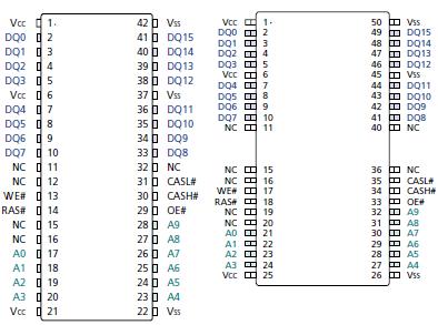 SpecificationsVoltage on VCC Pin Relative to VSS
3.3V ........................................................................... -1V to +4.6V
5V .............................................................................. -1V TO +7V
Voltage on NC, Inputs or I/O Pins Relative to VSS
3.3V ........................................................................... -1V to +5.5V
5V .............................................................................. -1V TO +7V
Operating Temperature
TA (commercial) .......................................................... 0°C to +70°C
TA (extended "ET") ..................................................... -20°C to +80°C
Storage Temperature (plastic) ..................................... -55°C to +150°C
Power Dissipation ........................................................ 1W
*Stresses greater than those listed under "Absolute Maximum Ratings" may cause permanent damage to the device. This is a stress rating only, and functional operation of the device at these or any other conditions above those indicated in the operational sections of this specification is not implied. Exposure to absolute maximum rating conditions for extended periods may affect reliability.DescriptionThe 1 Meg x 16 DRAM MT4LC1M16C3 is a randomly accessed, solidstate memory containing 16,777,216 bits organized in a x16 configuration. The 1 Meg x 16 DRAM has both BYTE WRITE and WORD WRITE access cycles via two CAS# pins (CASL# and CASH#). These function identically to a single CAS# on other DRAMs in that either CASL# or CASH# will generate an internal CAS#.
The CAS# function and timing of MT4LC1M16C3 are determined by the first CAS# (CASL# or CASH#) to transition LOW and the last CAS# to transition back HIGH. Use of only one of the two results in a BYTE access cycle. CASL# transitioning LOW selects an access cycle for the lower byte (DQ0-DQ7), and CASH# transitioning LOW selects an access cycle for the upper byte (DQ8-DQ15).
Each bit is uniquely addressed through the 20 address bits during READ or WRITE cycles. These are entered ten bits (A0-A9) at a time. RAS# is used to latch the first ten bits and CAS# the latter ten bits. The CAS# function is determined by the first CAS# (CASL# or CASH#) to transition LOW and the last one to transition back HIGH. The CAS# function also determines whether the cycle will be a refresh cycle (RAS#-ONLY) or an active cycle (READ, WRITE, or READ-WRITE) once RAS# goes LOW.
The CASL# and CASH# inputs of MT4LC1M16C3 internally generate a CAS# signal that functions identically to a single CAS# input on other DRAMs. The key difference is that each CAS# input (CASL# and CASH#) controls its corre- sponding DQ tristate logic (in conjunction with OE# and WE#). CASL# controls DQ0-DQ7 and CASH# controls DQ8-DQ15. The two CAS# controls give the 1 Meg x 16 DRAM BYTE WRITE cycle capabilities.
A logic HIGH on WE# of MT4LC1M16C3 dictates read mode, while a logic LOW on WE# dictates write mode. During a WRITE cycle, data-in (D) is latched by the falling edge of WE# or CAS, whichever occurs last. Taking WE# LOW will initiate a WRITE cycle, selecting DQ0-DQ15. If WE# goes LOW prior to CAS# going LOW, the output pin(s) remain open (High-Z) until the next CAS# cycle. If WE# goes LOW after CAS# goes LOW and data reaches the output pins, data-out (Q) of MT4LC1M16C3 is activated and retains the selected cell data as long as CAS# and OE# remain LOW (regardless of WE# or RAS#). This late WE# pulse results in a READ-WRITE cycle.
The 16 data inputs and 16 data outputs of MT4LC1M16C3 are routed through 16 pins using common I/O. Pin direction is controlled by OE# and WE#.

 MT4LC1M16C3 Data Sheet