Features: • Fast clock and OE# access times
• Single +3.3V ±0.165Vor 2.5V ±0.125V power supply (VDD)
• Separate +3.3V or 2.5V isolated output buffer supply (VDDQ)
• SNOOZE MODE for reduced-power standby
• Common data inputs and data outputs
• Individual BYTE WRITE control and GLOBAL WRITE
• Three chip enables for simple depth expansion and address pipelining
• Clock-controlled and registered addresses, data I/Os and control signals
• Internally self-timed WRITE cycle
• Burst control (interleaved or linear burst)
• Automatic power-down
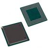
• 100-pin TQFP package
• 165-pin FBGA package
• Low capacitive bus loading
• x18, x32, and x36 versions availablePinout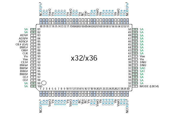
SpecificationsVoltage on VDD Supply
Relative to VSS .................................... -0.5V to +4.6V
Voltage on VDDQ Supply
Relative to VSS .................................... -0.5V to +4.6V
VIN (DQx) ...................................... -0.5V to VDDQ + 0.5V
VIN (inputs) ..................................... -0.5V to VDD + 0.5V
Storage Temperature (TQFP) ................ -55 to +150
Storage Temperature (FBGA) ................ -55 to +125
Junction Temperature** ...................................... +150
Short Circuit Output Current .................................100mA
Voltage on VDD Supply
Relative to VSS ..................................... -0.3V to +3.6V
Voltage on VDDQ Supply
Relative to VSS ..................................... -0.3V to +3.6V
VIN (DQx) ....................................... -0.3V to VDDQ + 0.3V
VIN (inputs) ...................................... -0.3V to VDD + 0.3V
Storage Temperature (TQFP) ................. -55 to +150
Storage Temperature (FBGA) ................. -55 to +125
Junction Temperature** ....................................... +150
Short Circuit Output Current ..................................100mA
*Stresses greater than those listed under "Absolute Maximum Ratings" may cause permanent damage to the device. This is a stress rating only, and functional operation of the device at these or any other conditions above those indicated in the operational sections of this specification is not implied. Exposure to absolute maximum rating conditions for extended periods may affect reliability.
**Maximum junction temperature depends upon package type, cycle time, loading, ambient temperature and airflow. See Micron Technical Note TN-05-14 for more information.
DescriptionThe Micron® SyncBurst™ SRAM family MT58V512V36D employs highspeed, low-power CMOS designs that are fabricated using an advanced CMOS process.
Micron's 16Mb SyncBurst SRAMs MT58V512V36D integrate a 1 Meg x 18, 512K x 32, or 512K x 36 SRAM core with advanced synchronous peripheral circuitry and a 2-bit burst counter. All synchronous inputs pass through registers controlled by a positive-edge-triggered single-clock input (CLK). The synchronous inputs of MT58V512V36D include all addresses, all data inputs, active LOW chip enable (CE#), two additional chip enables for easy depth expansion (CE2, CE2#), burst control inputs (ADSC#, ADSP#, ADV#), byte write enables (BWx#) and global write (GW#). Note that CE2# is not available on the T Version.
Asynchronous inputs of MT58V512V36D include the output enable (OE#), clock (CLK) and snooze enable (ZZ). There is also

 MT58V512V36D Data Sheet