MT70014

PinoutSpecificationsStorage Temperature - 65ºC to +150 Temperature (Ambient) under Bias - 55ºC to +125Supply Voltage VDD -0.3V to + 7VDC Input Voltage -0.3 to VDD +0.3VOutput Current (Single O/P) 10mAOutput Current (Total O/P) 20mADescriptionThe MT70014 consists of two independent channe...

product image

MT70014 Picture
SeekIC No. : 004430019 Detail

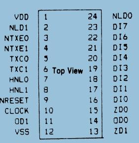
MT70014: PinoutSpecificationsStorage Temperature - 65ºC to +150 Temperature (Ambient) under Bias - 55ºC to +125Supply Voltage VDD -0.3V to + 7VDC Input Voltage -0.3 to VDD +0.3VOutput Current (Sing...

floor Price/Ceiling Price

Part Number:
MT70014
Supply Ability:
5000

Price Break

  • Qty
  • 1~5000
  • Unit Price
  • Negotiable
  • Processing time
  • 15 Days
Total Cost: $ 0.00

SeekIC Buyer Protection PLUS - newly updated for 2013!

  • Escrow Protection.
  • Guaranteed refunds.
  • Secure payments.
  • Learn more >>

Month Sales

268 Transactions

Rating

evaluate  (4.8 stars)

Upload time: 2024/4/28

Payment Methods

All payment methods are secure and covered by SeekIC Buyer Protection PLUS.

Notice: When you place an order, your payment is made to SeekIC and not to your seller. SeekIC only pays the seller after confirming you have received your order. We will also never share your payment details with your seller.
Product Details

Description


Pinout

  Connection Diagram


Specifications

Storage Temperature                                                 - 65ºC to +150
Temperature (Ambient) under Bias                             - 55ºC to +125
Supply Voltage VDD                                                          -0.3V to + 7V
DC Input Voltage                                                       -0.3 to VDD +0.3V
Output Current (Single O/P)                                                          10mA
Output Current (Total O/P)                                                            20mA


Description

The MT70014 consists of two independent channels each of which functions as a parallel to serial data converter.

The parallel data of MT70014 is loaded via an 8-bit input highway and the serial output is generated in the ARINC format, i.e. 31 bits of data plus one parity bit.

The input highway (DIO to D17) of MT70014  is common to both channels as are the reset (NRESET) CLOCK 9clock), positive supply (VDD), and ground (VSS) pins. Each channel has 3 control inputs. Channel 0 has a 'load' input (NLDO), a 'transmit enable' input (NTXEO), and a 'high/low speed' (HNLO) control input. There are 3 outputs per channel. Channel 0 has a 'data out zeros' (ZDO) output, a 'data out ones' (ODO) output and a'transmission complete' (TXCO) output. Operations for Channel 0 and Channel 1 are identical in all respects.

The data of MT70014 to be transmitted by a particular channel is loaded as four 8-bit bytes via the input highway.

The four bytes of MT70014 are stored on chip in the order in which they were loaded. Loading is performed by pulsing the (NLDO) input low. The data must then be changed to the value of the next byte and (NLDO) pulsed low again etc.

The four bytes of MT70014  are transmitted in the order in which they were loaded. The only exception is the most significant bit of the 4th byte. This bit is ignored and a parity bit is transmitted in its place.

The parity bit of MT70014 corresponds to an odd parity check on the first 31 bits, i.e. if the number of ones in the first 31 bits is odd, the parity bit is equal to zero.

Data of MT70014 is only accepted if the TXCO output is high. Once byte 4 has been loaded, TXCO is driven low. Data must be valid on the input highway for tsu before and to tH after the (NLDO) rising edge.

The clock (CLOCK) input of 5mhz + 1%* MT70014 is divided down on chip by 50 to give a serial data transmission rate for(HNLO) high or by 380 for (HNLO) low.

These rates of MT70014 correspond to the ARINC fast and slow rates respectively. The timing of the two output data lines (ODO)and (ZDO) is shown in Fig.2. A data value of one is signified by a positive pulse output on (ODO) and a zero by a positive pulse on (ZDO). The bit period tp will be 50/f CLK for (HNLO) high and 380/fCLK for (HNLO) low. * ARINC recommends that the transmission rate should not be precisely 100KHZ to avoid interference but any rate within +1% of these can be used.

The overall timing diagram for a complete data transfer MT70014 is shown in Fig.3. When the last byte has been loaded (TXCO) goes low. This signal is combined with the output of an on chip latch which is set by the (NTXEO) signal to initiate the start of transmission. The latch is reset upon start of transmission.

If the (NTXEO) signal of MT70014 is left permanently low the on chip latch is always set and transmission will be initiated by TXCO going low, i.e. as soon as the 4 bytes have been loaded. Hence there is an option between auto-start and controlled-start of transmission. At the end of the transmission TXCO goes high and the device is able to accept new data.

The MT70014 can be completely reset by pulsing the (NRESET) line low. This causes both channels to be put into the data load phase of operation. The TXC lines are forced high and all data outputs are forced low. the timing is shown in Fig. 4.


Customers Who Bought This Item Also Bought

Margin,quality,low-cost products with low minimum orders. Secure your online payments with SeekIC Buyer Protection.
LED Products
Soldering, Desoldering, Rework Products
Hardware, Fasteners, Accessories
Integrated Circuits (ICs)
Potentiometers, Variable Resistors
View more