Position: Home > Datasheet list > MX2 Series > Index M > MX25V8005
Electronica China

Purchase MX25V8005, In-stock MX25V8005 From SeekIC.


MX25V8005 Product Image

MX2 Series Datasheet download

Five Points

Part Number: MX25V8005


Description: The MX25V8005 is a CMOS 8,388,608 bit serial Flash memory, which is configured as 1,048,576 x 8 intern...


Urgent Purchase

MX25V8005 General Description


The MX25V8005 is a CMOS 8,388,608 bit serial Flash memory, which is configured as 1,048,576 x 8 internally. The MX25V8005 feature a serial peripheral interface and software protocol allowing operation on a simple 3-wire bus. The three bus signals are a clock input (SCLK), a serial data input (SI), and a serial data output (SO). SPI access to the device is enabled by CS# input.

The MX25V8005 provide sequential read operation on whole chip.After program/erase command is issued, auto program/ erase algorithms which program/ erase and verify the specified page or byte /sector/block locations will be executed. Program command is executed on page (256 bytes) basis, and erase command is executes on chip or sector(4K-byte) or block(64K-byte).

To provide user with ease of interface, a status register is included to indicate the status of the chip. The status read command can be issued to detect completion status of a program or erase operation via WIP bit.

When the device is not in operation and CS# is high, it is put in standby mode and draws less than 10uA DC current. The MX25V8005 utilize MXIC's proprietary memory cell, which reliably stores memory contents even after 100,000 program and erase cycles.

MX25V8005 Maximum Ratings

Ambient Operating Temperature ..............-40 to 85
Storage Temperature............................. -55 to 125
Applied Input Voltage............................... -0.5V to 4.6V
Applied Output Voltage............................ -0.5V to 4.6V
VCC to Ground Potential.......................... -0.5V to 4.6V
Notes:
1. Stresses greater than those listed under ABSOLUTE MAXIMUM RATINGS may cause permanent damage to the device. This is stress rating only and functional operational sections of this specification is not implied. Exposure to absolute maximum rating conditions for extended period may affect reliability.
2. Specifications contained within the following tables are subject to change.
3. During voltage transitions, all pins may overshoot to 4.0V or -0.5V for period up to 20ns.
4. All input and output pins may overshoot to VCC+0.5V while VCC+0.5V is smaller than or equal to 4.6V.

MX25V8005 Features

GENERAL
• Serial Peripheral Interface (SPI) compatible -- Mode 0 and Mode 3
• 8,388,608 x 1 bit structure
• 256 Equal Sectors with 4K byte each
- Any Sector can be erased individually
• 16 Equal Blocks with 64K byte each
- Any Block can be erased individually
• Single Power Supply Operation
- 2.35 to 3.6 volt for read, erase, and program operations
• Latch-up protected to 100mA from -1V to Vcc +1V
• Low Vcc write inhibit is from 1.5V to 2.2V
PERFORMANCE
• High Performance
- Fast access time: 50MHz serial clock
- Fast program time: 1.4ms(typ.) and 5ms(max.)/page (256-byte per page)
- Fast erase time: 60ms(typ.) and 120ms(max.)/sector (4K-byte per sector) ; 1s(typ.) and 2s(max.)/block (64K-byte per
block)
• Low Power Consumption
- Low active read current: 8mA(max.) at 50MHz and 4mA(max.) at 25MHz
- Low active programming current: 15mA (max.)
- Low active erase current: 15mA (max.)
- Low standby current: 10uA (max.)
• Minimum 100,000 erase/program cycles
• 10 years data retention
SOFTWARE FEATURES
• Input Data Format
- 1-byte Command code
• Block Lock protection
- The BP0~BP2 status bit defines the size of the area to be software protected against Program and Erase instructions.
• Auto Erase and Auto Program Algorithm
- Automatically erases and verifies data at selected sector
- Automatically programs and verifies data at selected page by an internal algorithm that automatically times the program pulse widths (Any page to be programed should have page in the erased state first)
• Status Register Feature
• Electronic Identification
- JEDEC 2-byte Device ID
- RES command, 1-byte Device ID
HARDWARE FEATURES
• SCLK Input
- Serial clock input
• SI Input
- Serial Data Input
• SO Output
- Serial Data Output
• WP# pin
- Hardware write protection
• HOLD# pin
- pause the chip without diselecting the chip
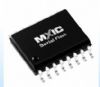
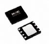
• PACKAGE
- 8-pin SOP (150mil)
- 8-land WSON (6x5mm)
- All Pb-free devices are RoHS Compliant

MX25V8005 Connection Diagram

MX25V8005  Connection Diagram

MX25V8005 datasheet

MX205Q
PDF/DataSheet Download

Find MX25V8005 Suppliers

  • ·MX205QC
  • ETC [ETC] 
  • Low Cost, 5.0g, Dual Axis Accelerometer with Analog Outputs 
  • 252911 KB
  • MX205QC Datasheet Download
  • ·MX205QL
  • ETC [ETC] 
  • Low Cost, 5.0g, Dual Axis Accelerometer with Analog Outputs 
  • 252911 KB
  • MX205QL Datasheet Download
  • ·MX210Q
  • ETC [ETC] 
  • Low Cost, 10g, Dual Axis Accelerometer with Analog Outputs 
  • 252922 KB
  • MX210Q Datasheet Download
  • ·MX210QC
  • ETC [ETC] 
  • Low Cost, 10g, Dual Axis Accelerometer with Analog Outputs 
  • 252922 KB
  • MX210QC Datasheet Download
  • ·MX210QL
  • ETC [ETC] 
  • Low Cost, 10g, Dual Axis Accelerometer with Analog Outputs 
  • 252922 KB
  • MX210QL Datasheet Download
  • ·MX214
  • CMLMICRO [CML Microcircuits] 
  • Variable Split Band Inverter 
  • 238010 KB
  • MX214 Datasheet Download
  • ·MX23C1010
  • MCNIX [Macronix International] 
  • 1M-BIT MASK ROM (8 BIT OUTPUT) 
  • 119262 KB
  • MX23C1010 Datasheet Download
  • ·MX23C1010MC-10
  • MCNIX [Macronix International] 
  • 1M-BIT MASK ROM (8 BIT OUTPUT) 
  • 119262 KB
  • MX23C1010MC-10 Datasheet Download

MX25V8005 Relative Products

  • MX25V512

    MX25V512

    The MX25V512 is a CMOS 524,288 bit serial Flash memory, which is configured as 65,536 x 8 internally. The MX25V512 feature a serial peripheral interface and software protocol allowing operation on a simple 3-wire bus. The three bus signals are a clock input ...

  • MX25V4035

    MX25V4035

    The MX25V4035 are 4,194,304 bit serial Flash memory, which is configured as 524,288 x 8 internally. When it is in two or four I/O read mode, the structure becomes 2,097,152 bits x 2 or 1,048,576 bits x 4. The MX25V8035 are 8,388,608 bit serial Flash memory, ...

  • MX25U4035

    MX25U4035

    The MX25U4035 are 4,194,304 bit serial Flash memory, which is configured as 524,288 x 8 internally. When it is in two or four I/O read mode, the structure becomes 2,097,152 bits x 2 or 1,048,576 bits x 4. The MX25U8035 are 8,388,608 bit serial Flash memory, ...

  • MX25L6405D

    MX25L6405D

    The MX25L1605D are 16,777,216 bit serial Flash memory, which is configured as 2,097,152 x 8 internally. When it is in two I/O read mode, the structure becomes 8,388,608 bits x 2. The MX25L3205D are 33,554,432 bit serial Flash memory, which is configured as 4...

  • MX25L4004

    MX25L4004

    The MX25L4004 is a CMOS 4,390,912 bit serial Flash EEPROM, which is configured as 548,864 x 8 internally.The MX25L4004 features a serial peripheral interface and software protocal allowing operation on a simple 3- wire bus. The three bus signals are a clock ...

  • MX25L3235D

    MX25L3235D

    The MX25L3235D are 32,554,432 bit serial Flash memory, which is configured as 4,194,304 x 8 internally. When it is in two or four I/O read mode, the structure becomes 16,777,216 bits x 2 or 8,388,608 bits x 4. The MX25L3235D feature a serial peripheral inter...

Hotspot Suppliers Product

  • Models: G6B-1114P-US
Price: 1.75-2 USD

    G6B-1114P-US

    Price: 1.75-2 USD

    RELAY GEN PURPOSE SPST 5A 12V - G6B-1114P-US

  • Models: 24LC08B
Price: 0.13-0.18 USD

    24LC08B

    Price: 0.13-0.18 USD

    8K, I2C Serial EEPROM, 400KHz, 8SOIC, 2-wire serial interface, Low-Power CMOS Technology

  • Models: TSB41LV06APZPG4
Price: 9.4-9.9 USD

    TSB41LV06APZPG4

    Price: 9.4-9.9 USD

    100-HTQFP, digital and analog transceiver, -0.3V to 4V, Ultra low Power Sleep Mode, link layer con...

  • Models: S29GL032N90TFI040
Price: 0.9-1.3 USD

    S29GL032N90TFI040

    Price: 0.9-1.3 USD

    3.0-Volt single-power Flash memory, TSOP, –0.5 V to +4.0 V, 200 mA, Single power supply operation

  • Models: CD54HC30F3A
Price: 1-10 USD

    CD54HC30F3A

    Price: 1-10 USD

    CERDIP, NAND Gate, 2V

  • Models: EP610ILI-12
Price: 12.5-14 USD

    EP610ILI-12

    Price: 12.5-14 USD

    EPLD, PLCC, –2.0 to 7.0V

  • Models: OP191GSZ-REEL7
Price: 0.93-1.2 USD

    OP191GSZ-REEL7

    Price: 0.93-1.2 USD

    IC OPAMP GP R-R 3MHZ 16MA 8SOIC - OP191GSZ-REEL7

  • Models: LM98513CCMT
Price: 3.5-6.5 USD

    LM98513CCMT

    Price: 3.5-6.5 USD

    56-TSSOP, 3 Volt Single Power Supply, Low Power CMOS Design, Dual-Channel, Copier Signal Processor

  • Models: APA4838
Price: 0.9-1.2 USD

    APA4838

    Price: 0.9-1.2 USD

    2.8W Audio Power Amplifier, 4.5V to 5V, TSSOP-28, 0dB to -78dB, 0.7μA, 32Ω

  • Models: RC4558DRG4
Price: 0.8-1 USD

    RC4558DRG4

    Price: 0.8-1 USD

    dual general-purpose operational amplifier, 3MHZ, 8SOIC, 18 V, RC4558DRG4

  • Models: TWL2214CAPFBR
Price: 1-1 USD

    TWL2214CAPFBR

    Price: 1-1 USD

    single-chip battery, Battery Temperature Sensing, 48-Terminal Plastic TQFP (PFB)

  • Models: RJ017
Price: 1-4 USD

    RJ017

    Price: 1-4 USD

    QFP, 15000 pps, chip bidge, highly intergrated ASIC, 6.0V

Map list:   ABCDEFGHIJKLMNOPQRSTUVWXYZ    0123456789All