NBSG53A

Features: • Maximum Input Clock Frequency (DFF) > 8 GHz Typical (See Figures 4, 6, 8, 10, and 11)• Maximum Input Clock Frequency (DIV/2) > 10 GHz Typical (See Figures 5, 7, 9, 10, and 11)• 210 ps Typical Propagation Delay (OLS = FLOAT)• 45 ps Typical Rise and Fall Tim...

product image

NBSG53A Picture
SeekIC No. : 004432750 Detail

NBSG53A: Features: • Maximum Input Clock Frequency (DFF) > 8 GHz Typical (See Figures 4, 6, 8, 10, and 11)• Maximum Input Clock Frequency (DIV/2) > 10 GHz Typical (See Figures 5, 7, 9, 10, ...

floor Price/Ceiling Price

Part Number:
NBSG53A
Supply Ability:
5000

Price Break

  • Qty
  • 1~5000
  • Unit Price
  • Negotiable
  • Processing time
  • 15 Days
Total Cost: $ 0.00

SeekIC Buyer Protection PLUS - newly updated for 2013!

  • Escrow Protection.
  • Guaranteed refunds.
  • Secure payments.
  • Learn more >>

Month Sales

268 Transactions

Rating

evaluate  (4.8 stars)

Upload time: 2024/5/2

Payment Methods

All payment methods are secure and covered by SeekIC Buyer Protection PLUS.

Notice: When you place an order, your payment is made to SeekIC and not to your seller. SeekIC only pays the seller after confirming you have received your order. We will also never share your payment details with your seller.
Product Details

Description


Features:

• Maximum Input Clock Frequency (DFF) > 8 GHz Typical (See Figures 4, 6, 8, 10, and 11)
• Maximum Input Clock Frequency (DIV/2) > 10 GHz Typical (See Figures 5, 7, 9, 10, and 11)
• 210 ps Typical Propagation Delay (OLS = FLOAT)
• 45 ps Typical Rise and Fall Times (OLS = FLOAT)
• DIV/2 Mode (Active with Select Low)
• DFF Mode (Active with Select High)
• Selectable Swing PECL Output with Operating Range: VCC = 2.375 V to 3.465 V with VEE = 0 V
• Selectable Swing NECL Output with NECL Inputs with Operating Range: VCC = 0 V with VEE = −2.375 V to −3.465 V
• Selectable Output Level (0 V, 200 mV, 400 mV, 600 mV, or 800 mV Peak−to−Peak Output)
• 50 Internal Input Termination Resistors on all Differential Inputs *Output Level Select


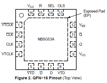
Pinout

  Connection Diagram


Specifications

Symbol
Parameter
Condition 1 Condition 2
Rating
Units
VCC
LVPECL Power Supply

VEE = 0 V

 
3.6
V
VEE
NECL Power Supply VCC = 0 V  
-3.6
V
VI
Positive Input
Negative Input
VEE = 0 V
VCC = 0 V
VI VCC
VI VEE
3.6
-3.6
V
V
VINPP
Differential Input Voltage |D-D| VCC - VEE 2.8
VCC - VEE < 2.8

 
2.8
|VCC-VEE|
V
V
IIN
Input Current Through RT (50 Resistor) Static
Surge
 
45
80
V
V
Iout
Output Current Continuous
Surge
 
25
50
mA
mA
TA
Operating Temperature Range 16 FCBGA
16 QFN
 
-40 to +70
-40 to +85
Tstg
Storage Temperature Range    
-65 to +150
JA
Thermal Resistance (Junction-to-Ambient)
(Note6)
0 LFPM
500 LFPM
0 LFPM
500 LFPM
16 FCBGA
16 FCBGA
16 QFN
16 QFN
108
86
41.6
35.2
/W
/W
/W
/W
JC
Thermal Resistance (Junction-to-Case) 2S2P (Note 6)
2S2P (Note 7)
16 FCBGA
16 QFN
5.0
4.0
/W
/W
Tsol
Wave Solder < 15 Seconds  
225


Maximum ratings are those values beyond which device damage can occur. Maximum ratings applied to the device are  ndividual stress limit values (not normal operating conditions) and are not valid simultaneously. If these limits are exceeded, device  unctional operation is not implied, damage may occur and reliability may be affected.
6. JEDEC standard 51−6, multilayer board − 2S2P (2 signal, 2 power).
7. JEDEC standard multilayer board − 2S2P (2 signal, 2 power) with 8 filled thermal vias under exposed pad.


Description

The NBSG53A is a multi−function differential D flip−flop (DFF) or fixed divide by two (DIV/2) clock generator. This is a part of the GigaComm] family of high performance Silicon Germanium products. A strappable control pin is provided to select between the two functions. The device is housed in a low profile 4x4 mm 16−pin Flip−Chip BGA (FCBGA) or a 3x3 mm 16 pin QFN package.

The NBSG53A is a device with data, clock, OLS, reset, and select inputs. Differential inputs incorporate internal 50 termination resistors and accept NECL (Negative ECL), PECL (Positive ECL), LVCMOS/LVTTL, CML, or LVDS. The OLS input is used to program the peak−to−peak output amplitude between 0 and 800 mV in five discrete steps. The RESET and SELECT inputs are single−ended and can be driven with either LVECL or LVCMOS/LVTTL input levels.

Data is transferred to the outputs on the positive edge of the clock. The differential clock inputs of the NBSG53A allow the device to also be used as a negative edge triggered device.


Customers Who Bought This Item Also Bought

Margin,quality,low-cost products with low minimum orders. Secure your online payments with SeekIC Buyer Protection.
Sensors, Transducers
Integrated Circuits (ICs)
Cables, Wires
Industrial Controls, Meters
Connectors, Interconnects
View more