Configuration
: Single
Maximum Operating Temperature
: + 175 C
Mounting Style
: Through Hole
Transistor Polarity
: P-Channel
Packaging
: Tube
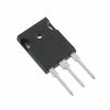
Package / Case
: TO-220
Continuous Drain Current
: 30 A
Drain-Source Breakdown Voltage
: - 30 V
Resistance Drain-Source RDS (on)
: 0.025 Ohms
Gate-Source Breakdown Voltage
: +/- 16 V
Features: `-30 A, -30 V. RDS(ON) = 0.042 @ VGS= -4.5 V
RDS(ON) = 0.025 @ VGS= -10 V.
`Critical DC electrical parameters specified at elevated temperature.
`Rugged internal source-drain diode can eliminate the need for an external Zener diode transient suppressor.
`High density cell design for extremely low RDS(ON).
`175°C maximum junction temperature rating.Specifications
|
Symbol |
Parameter |
NDP6030PL |
NDB6030PL |
Units |
| VDSS |
Drain-Source Voltage |
-30 |
V |
| VGSS |
Gate-Source Voltage - Continuous |
± 16 |
V |
| ID |
Drain Current - Continuous
- Pulsed |
-30 |
A |
|
-90 |
| PD |
Total Power Dissipation @ TC = 25°C
Derate above 25°C |
75 |
W |
|
0.5 |
W/ |
| TJ,TSTG |
Operating and Storage Temperature Range |
-65 to 175 |
|
| TL |
Maximum lead temperature for soldering purposes, 1/8" from case for 5 seconds |
275 |
|
| TJ,TSTG |
Operating and Storage Temperature Range |
-65 to 175 |
|
DescriptionThese P-Channel logic level enhancement mode power field effect transistors NDP6030PL are produced using Fairchild's proprietary, high cell density, DMOS technology. This very high density process is especially tailored to minimize on-state resistance. NDP6030PL is particularly suited for low voltage applications such as DC/DC converters and high efficiency switching circuits where fast switching, low in-line power loss, and resistance to transients are needed.
Parameters: | Technical/Catalog Information | NDP6030PL |
| Vendor | Fairchild Semiconductor |
| Category | Discrete Semiconductor Products |
| Mounting Type | Through Hole |
| FET Polarity | P-Channel |
| Drain to Source Voltage (Vdss) | 30V |
| Current - Continuous Drain (Id) @ 25° C | 30A |
| Rds On (Max) @ Id, Vgs | 25 mOhm @ 19A, 10V |
| Input Capacitance (Ciss) @ Vds | 1570pF @ 15V |
| Power - Max | 75W |
| Packaging | Tube |
| Gate Charge (Qg) @ Vgs | 36nC @ 5V |
| Package / Case | TO-220 |
| FET Feature | Logic Level Gate |
| Lead Free Status | Lead Free |
| RoHS Status | RoHS Compliant |
| Other Names | NDP6030PL
NDP6030PL
|

 NDP6030PL Data Sheet