Features: • Single Pulsed RAS Interface
• Fully Synchronous to Positive Clock Edge
• Four Banks controlled by BS0/BS1 (Bank Select)
• Programmable CAS Latency: 2, 3
• Programmable Burst Length: 1, 2, 4, 8, Full page
• Programmable Wrap: Sequential or Interleave
• Multiple Burst Read with Single Write Option
• Automatic and Controlled Precharge Command
• Data Mask for Read/Write control (x4, x8)
• Dual Data Mask for byte control (x16)
• Auto Refresh (CBR) and Self Refresh
• Suspend Mode and Power Down Mode
• Standard Power operation
• 4096 refresh cycles/64ms
• Random Column Address every CK (1-N Rule)
• Single 3.3V ± 0.3V Power Supply
• LVTTL compatible
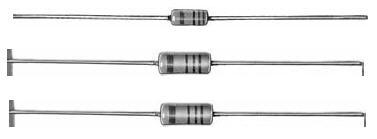
• Package: 54-pin 400 mil TSOP-Type IIPinout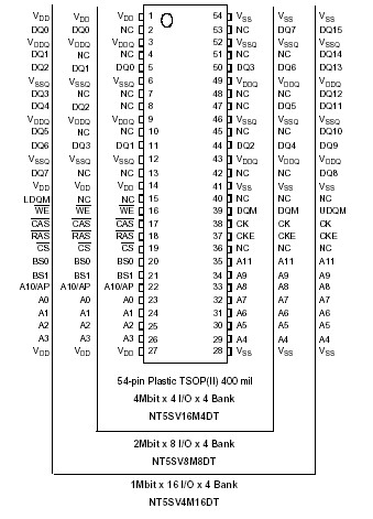 Specifications
| Symbol |
Parameter |
Rating |
Units |
Notes |
| VDD |
Power Supply Voltage |
-0.3 to +4.6 |
V |
1 |
| VDDQ |
Power Supply Voltage for Output |
-0.3 to +4.6 |
V |
1 |
| VIN |
Input Voltage |
-0.3 to VDD+0.3 |
V |
1 |
| VOUT |
Output Voltage |
-0.3 to VDD+0.3 |
V |
1 |
| TA |
Operating Temperature (ambient) |
0 to +70 |
°C |
1 |
| TSTG |
Storage Temperature |
-55 to +125 |
°C |
1 |
| PD |
Power Dissipation |
1.0 |
W |
1 |
| IOUT |
Short Circuit Output Current |
50 |
mA |
1 |
DescriptionThe NT5SV16M4DT, NT5SV8M8DT, and NT5SV4M16DT are four-bank Synchronous DRAMs organized as 4Mbit x 4 I/O x 4 Bank, 2Mbit x 8 I/O x 4 Bank, and 1Mbit x 16 I/O x 4 Bank, respectively. These synchronous devices achieve high-speed data transfer rates of up to 200MHz by employing a pipeline chip architecture that synchronizes the output data to a system clock. The chip is fabricated with NTC's advanced 64Mbit single transistor CMOS DRAM process technology.
The device NT5SV4M16DT is designed to comply with all JEDEC standards set for synchronous DRAM products, both electrically and mechanically. All of the control, address, and data input/output (I/O or DQ) circuits are synchronized with the positive edge of an externally supplied clock.
RAS, CAS, WE, and CS are pulsed signals which are examined at the positive edge of each externally applied clock (CK). NT5SV4M16DT Internal chip operating modes are defined by combinations of these signals and a command decoder initiates the necessary timings for each operation. A fourteen bit address bus accepts address data in the conventional RAS/CAS multiplexing style. Twelve row addresses (A0-A11) and two bank select addresses (BS0, BS1) are strobed with RAS. Eleven column addresses (A0-A9) plus bank select addresses and A10 are strobed with CAS. Column address A9 is dropped on the x8 device, and column addresses A8 and A9 are dropped on the x16 device.
Prior to any access operation, the CAS latency, burst length, and burst sequence must be programmed into the device NT5SV4M16DT by address inputs A0-A11, BS0, BS1 during a mode register set cycle. In addition, it is possible to program a multiple burst sequence with single write cycle for write through cache operation.
Operating the four memory banks in an interleave fashion allows random access operation to occur at a higher rate than is possible with standard DRAMs. A sequential and gapless data rate of up to 200MHz is possible depending on burst length, CAS latency, and speed grade of the device NT5SV4M16DT.Simultaneous operation of both decks of a stacked device is allowed, depending on the operation being done. Auto Refresh (CBR) and Self Refresh operation are supported.

 NT5SV4M16DT Data Sheet