Transistor Polarity
: N-Channel
Gate-Source Breakdown Voltage
: +/- 20 V
Configuration
: Single
Maximum Operating Temperature
: + 175 C
Mounting Style
: SMD/SMT
Package / Case
: DPAK
Packaging
: Tube
Resistance Drain-Source RDS (on)
: 4.6 mOhms
Continuous Drain Current
: 32 A
Drain-Source Breakdown Voltage
: 24 V
Features: • Planar HD3e Process for Fast Switching Performance
• Low RDS(on) to Minimize Conduction Loss
• Low Ciss to Minimize Driver Loss
• Low Gate Charge
• Optimized for High Side Switching Requirements in
High−Efficiency DC−DC Converters
• Pb−Free Packages are AvailablePinout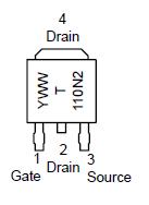 Specifications
| Rating |
Symbol |
Value |
Unit |
| Drain−to−Source Voltage |
VDSS |
24 |
V |
| Gate−to−Source Voltage − Continuous |
VGS |
±20 |
V |
Thermal Resistance − Junction−to−Case
Total Power Dissipation @ TC = 25°C
Drain Current
− Continuous @ TC = 25°C, Chip
− Continuous @ TC = 25°C,
Limited by Package
− Continuous @ TA = 25°C,
Limited by Wires
− Single Pulse (tp = 10 �s) |
RJC
PD
ID
ID
ID
ID |
1.35
110
110
110
32
110 |
°C/W
W
A
A
A
A |
Thermal Resistance
− Junction−to−Ambient (Note 1)
− Total Power Dissipation @ TA = 25°C
− Drain Current − Continuous @ TA = 25°C |
RJA
PD
ID |
52
2.88
17.5 |
°C/W
W
A |
Thermal Resistance
− Junction−to−Ambient (Note 2)
− Total Power Dissipation @ TA = 25°C
− Drain Current − Continuous @ TA = 25°C |
RJA
PD
ID |
100
1.5
12.5 |
°C/W
W
A |
Operating and Storage
Temperature Range |
TJ, Tstg |
−55 to 175 |
°C |
|
Single Pulse Drain−to−Source Avalanche
Energy − Starting TJ = 25°C
(VDD = 50 Vdc, VGS = 10 Vdc,
IL = 15.5 Apk, L = 1.0 mH, RG = 25 ) |
EAS |
120 |
|
Maximum Lead Temperature for Soldering
Purposes, (1/8", from case for 10 s) |
|
260 |
°C |
Maximum ratings are those values beyond which device damage can occur. Maximum ratings applied to the device are individual stress limit values (not normal operating conditions) and are not valid simultaneously. If these limits are exceeded, device functional operation is not implied, damage may occur and reliability may be affected.
1. When surface mounted to an FR4 board using 0.5 sq in drain pad size.
2. When surface mounted to an FR4 board using the minimum recommended pad size.DescriptionThe NTD110N02R is a power MOSFET 24 V, 110 A, N-channel DPAK.In no event shall Sensitron Semiconductor be liable for any damages that may result from an accident or any other cause during operation of the user's units according to the datasheet(s). Sensitron Semiconductor of NTD110N02R assumes no responsibility for any intellectual property claims or any other problems that may result from applications of information, products or circuits described in the datasheets.
Features of the NTD110N02R are:(1)planar HD3e process for fast switching performance; (2)low RDS(on) to minimize conduction loss; (3)low Ciss to minimize driver loss; (4)low gate charge; (5)optimized for high side switching requirements in high-efficiency DC-DC converters; (6)Pb-free packages are available.
The absolute maximum ratings of the NTD110N02R can be summarized as:(1)drain-to-source voltage:24 V;(2)storage temperature range:-55 to 175;(3)gate-to-source voltage:±20V;(4)operating temperature:-55 to 175;(5)continuous drain current:110A.Maximum ratings are those values beyond which device damage can occur.Maximum ratings applied to the device are individual stress limit values (not normal operating conditions) and are not valid simultaneously. If these limits are exceeded, device functional operation of NTD110N02R is not implied, damage may occur and reliability may be affected.SCILLC reserves the right to make changes without further notice to any products herein. SCILLC makes no warranty, representation or guarantee regarding the suitability of its products for any particular purpose, nor does SCILLC assume any liability arising out of the application or use of any product or circuit, and specifically disclaims any and all liability, including without limitation special, consequential or incidental damages."Typical" parameters which may be provided in SCILLC data sheets and/or specifications can and do vary in different applications and actual performance may vary over time.All operating parameters, including "Typicals" must be validated for each customer application by customer's technical experts.
At present there is not too much information about this model.If you are willing to find more about NTD110N02R, please pay attention to our web! We will promptly update the relevant information.

 NTD110N02R Data Sheet


