Features: ` OMAP3515/03 Applications Processor:
OMAP™ 3 Architecture
MPU Subsystem
` 600-MHz ARM Cortex™-A8 Core
` NEON™ SIMD Coprocessor
2D/3D Graphics Accelerator (OMAP3515 Device Only)
` Tile Based Architecture Delivering up 10 MPoly/sec
` Universal Scalable Shader Engine: Multi-threaded Engine Incorporating Pixel and Vertex Shader Functionality
` Industry Standard API Support: OpenGLES 1.1 and 2.0, OpenVG1.0 and Direct3D Mobile
` Fine Grained Task Switching, Load Balancing, and Power Management
` Programmable High Quality Image Anti-Aliasing
Fully Software-Compatible With ARM9™
Commercial and Extended Temperature Grades
` ARM Cortex™-A8 Core
ARMv7 Architecture
` Trust Zone®
` Thumb®-2
` MMU Enhancements
In-Order, Dual-Issue, Superscalar Microprocessor Core
NEON™ Multimedia Architecture
Over 2x Performance of ARMv6 SIMD
Supports Both Integer and Floating Point SIMD
Jazelle® RCT Execution Environment Architecture
Dynamic Branch Prediction with Branch Target Address Cache, Global History Buffer, and 8-Entry Return Stack
Embedded Trace Macrocell (ETM) Support for Non-Invasive Debug
` ARM Cortex™-A8 Memory Architecture:
16K-Byte Instruction Cache (4-Way Set-Associative)
16K-Byte Data Cache (4-Way Set-Associative)
256K-Byte L2 Cache
` 112K-Byte ROM
` 64K-Byte Shared SRAM
` Endianess:
ARM Instructions - Little Endian
ARM Data Configurable
` External Memory Interfaces:
SDRAM Controller (SDRC)
` 16, 32-bit Memory Controller With 1G-Byte Total Address Space
` Interfaces to Low-Power Double Data Rate (LPDDR) SDRAM
` SDRAM Memory Scheduler (SMS) and Rotation Engine
General Purpose Memory Controller (GPMC)
` 16-bit Wide Multiplexed Address/Data Bus
` Up to 8 Chip Select Pins With 128M-Byte Address Space per Chip Select Pin
` Glueless Interface to NOR Flash, NAND Flash (With ECC Hamming Code Calculation), SRAM and Pseudo-SRAM
` Flexible Asynchronous Protocol Control for Interface to Custom Logic (FPGA,CPLD, ASICs, etc.)
` Nonmultiplexed Address/Data Mode (Limited 2K-Byte Address Space)
` System Direct Memory Access (sDMA) Controller (32 Logical Channels With Configurable Priority)
` Camera Image Signal Processing (ISP)
CCD and CMOS Imager Interface
Memory Data Input
RAW Data Interface
BT.601/BT.656 Digital YCbCr 4:2:2 (8-/16-Bit) Interface
A-Law Compression and Decompression
Preview Engine for Real-Time Image Processing
Glueless Interface to Common Video Decoders
Histogram Module/Auto-Exposure,Auto-White Balance, and Auto-Focus Engine
Resize Engine
` Resize Images From 1/4x to 4x
` Separate Horizontal/Vertical Control
` Display Subsystem
Parallel Digital Output
` Up to 24-Bit RGB
` HD Maximum Resolution
` Supports Up to 2 LCD Panels
` Support for Remote Frame Buffer Interface (RFBI) LCD Panels
2 10-Bit Digital-to-Analog Converters (DACs) Supporting:
` Composite NTSC/PAL Video
` Luma/Chroma Separate Video (S-Video)
Rotation 90-, 180-, and 270-degrees
Resize Images From 1/4x to 8x Color Space Converter
8-bit Alpha Blending
` Serial Communication
5 Multichannel Buffered Serial Ports (McBSPs)
` 512 Byte Transmit/Receive Buffer (McBSP1/3/4/5)
` 5K-Byte Transmit/Receive Buffer (McBSP2)
` SIDETONE Core Support (McBSP2 and 3 Only) For Filter, Gain, and Mix Operations
` Direct Interface to I2S and PCM Device and TDM Buses
` 128 Channel Transmit/Receive Mode
Four Master/Slave Multichannel Serial Port Interface (McSPI) Ports
High-Speed/Full-Speed/Low-Speed USB OTG Subsystem (12-/8-Pin ULPI Interface)
High-Speed/Full-Speed/Low-Speed Multiport USB Host Subsystem
` 12-/8-Pin ULPI Interface or 6-/4-/3-Pin Serial Interface
` Supports Transceiverless Link Logic (TLL)
One HDQ/1-Wire Interface
Three UARTs (One with Infrared Data Association [IrDA] and Consumer Infrared [CIR] Modes)
Three Master/Slave High-Speed Inter-Integrated Circuit (I2C) Controllers
` Removable Media Interfaces:
Three Multimedia Card (MMC)/ Secure Digital (SD) With Secure Data I/O (SDIO)
` Comprehensive Power, Reset, and Clock Management
SmartReflex™ Technology
Dynamic Voltage and Frequency Scaling (DVFS)
` Test Interfaces
IEEE-1149.1 (JTAG) Boundary-Scan Compatible
Embedded Trace Macro Interface (ETM)
Serial Data Transport Interface (SDTI)
` 12 32-bit General Purpose Timers
` 2 32-bit Watchdog Timers
` 1 32-bit 32-kHz Sync Timer
` Up to 188 General-Purpose I/O (GPIO) Pins (Multiplexed With Other Device Functions)
` 65-nm CMOS Technology
` Package-On-Package (POP) Implementation for Memory Stacking (Not Available in CUS Package)
` Discrete Memory Interface (Not Available in CBC Package)
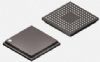
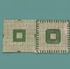
` Packages:
515-pin PBGA package (CBB Suffix), .5mm Ball Pitch (Top), .4mm Ball Pitch (Bottom)
515-pin S-PBGA package (CBC Suffix),.65mm Ball Pitch (Top), .5mm Ball Pitch (Bottom)
423-pin PBGA package (CUS Suffix), .65mm Ball Pitch
` 1.8-V I/O and 3.0-V (MMC1 only), 0.8-V to 1.35-V Adaptive Processor Core Voltage,0.8-V to 1.15-V Adaptive Core Logic Voltage
Application Portable Navigation Devices
Portable Media Player
Advanced Portable Consumer Electronics
Digital TV
Digital Video Camera
Portable Data Collection
Point-of-Sale Devices
Gaming
Web Tablet
Smart White Goods
Smart Home Controllers
Ultra Mobile DevicesSpecificationsThe following table specifies the absolute maximum ratings over the operating junction temperature range of OMAP commercial and extended temperature devices. Stresses beyond those listed under absolute maximum ratings may cause permanent damage to the device. These are stress ratings only and functional operation of the device at these or any other conditions beyond those indicated under recommended operating conditions is not implied. Exposure to absolute-maximum-rated conditions for extended periods may affect device reliability.
Notes:
` Logic functions and parameter values are not assured out of the range specified in the recommended operating conditions.
` The OMAP3515/03 device adheres to EIA/JESD22A114, Electrostatic Discharge (ESD) Sensitivity Testing Human Body Model (HBM). Minimum pass level for HBM is ±2 kV.
|
PARAMETER |
MIN |
MAX |
UNIT |
vdd_mpu
vdd_core |
Supply voltage range for core macros |
0.5 |
1.6 |
V |
vdds
vdds_mem |
Second supply voltage range for 1.8-V I/O macros |
0.5 |
2.25 |
vdds_mmc1
vdds_mmc1a |
Second supply voltage range for 1.8-V IOs |
0.5 |
2.45 |
| Second supply voltage range for 3.0-V IOs |
0.5 |
3.50 |
vdds_dsi
vdds_sdi
vdds_csi2
vdds_csib |
Supply voltage for DSI
Supply voltage for SDI
Supply voltage for CSI2
Supply voltage for CSIb |
0.5(1) |
2.10(1) |
vdds_dpll_dll
vdds_dpll_per |
Supply voltage for DLL DPLL
Supply voltage for Per DPLL |
0.5 |
2.10 |
vdds_sram
vdds_wkup_bg |
Supply voltage for SRAM LDOs
Supply voltage for wakeup LDO and VDDA (2 LDOs SRAM and BG) |
0.5 |
2.25 |
| VPAD |
Voltage range
at PAD |
CSIb (Balls K28, L28, K27, L27)
CSI2 (Balls AG17, AH17, AG19, AH19, AG18, AH18)
DSI (Balls AG22, AH22, AG23, AH23, AG24, AH24)
SDI (Balls AD28, AD27, AB28, AB27, AA28, AA27, AC27, AC28) |
0.5(1) |
2.10(1) |
| MMC1, MS (Balls N28, M27, N27, N26, N25, P28) MMC1, SIM (Balls P27, P26, R27, R25) |
Supply voltage range
for 1.8-V IOs |
0.54(2) |
2.34(2) |
Supply voltage range
for 3.0-V IOs |
0.45(3) |
3.45(3) |
| I2C1, I2C2, I2C3, I2C4 (Balls K21, J21, AF15, AE15, AF14, AG14, AD26, AE26) |
0.63(2) |
2.73(2) |
| Crystal (xtalin/xtalout) (Balls AE17, AF17) |
0.5 |
2.71 |
| Other balls |
0.5 |
vddsx(4) + 0.5 |
| vdda_dac |
Supply voltage range for analog macros |
0.5 |
2.43 |
| VESD |
ESD stress
voltage(5) |
HBM (human body model)(6) |
|
2000 |
| CDM (charged device model)(7) |
|
500 |
| IIOI |
Current-pulse injection on each I/O pin(8) |
|
200 |
mA |
| Iclamp |
Clamp current for an input or output |
-20 |
20 |
mA |
(1) To be confirmed.
(2) For a maximum time of 30% time period.
(3) For a maximum time of 15% time period.
(4) ) Depending on ball, vddsx can be vdds_mem or vdds.
(5) Electrostatic discharge (ESD) to measure device sensitivity/immunity to damage caused by electrostatic discharges into the device.
(6) JEDEC JESD22A114 D with the following exception-no connect pins are not stressed. 2000V Human Body Model (HBM)
(7) JEDEC JESD22C101C with the following exception-split out pin groupings to eliminate cumulative stress effect
(8) Each device is tested with I/O pin injection of 200 mA with a stress voltage of 1.5 times maximum vdd at room temperature.
DescriptionOMAP3515 and OMAP3503 high-performance, applications processors are based on the enhanced OMAP™ 3 architecture.
The OMAP™ 3 architecture is designed to provide best-in-class video, image, and graphics processing sufficient to support the following:
· Streaming video
· 2D/3D mobile gaming
· Video conferencing
· High-resolution still image
· Video capture in 2.5G wireless terminals, 3G wireless terminals, and rich multimedia-featured handsets, and high-performance personal digital assistants (PDAs).
The device supports high-level operating systems (OSs), such as:
· Windows CE
· Symbian OS
· Linux
· Palm OS
This OMAP device includes state-of-the-art power-management techniques required for high-performance mobile products.
The following subsystems are part of the device:
· Microprocessor unit (MPU) subsystem based on the ARM Cortex™-A8 microprocessor
· SGX subsystem for 2D and 3D graphics acceleration to support display and gaming effects (3515only)
· Camera image signal processor (ISP) that supports multiple formats and interfacing options connected to a wide variety of image sensors
· Display subsystem with a wide variety of features for multiple concurrent image manipulation, and a programmable interface supporting a wide variety of displays. The display subsystem also supports NTSC/PAL video out.
· Level 3 (L3) and level 4 (L4) interconnects that provide high-bandwidth data transfers for multiple initiators to the internal and external memory controllers and to on-chip peripherals The device also offers:
· A comprehensive power and clock-management scheme that enables high-performance, low-power operation, and ultralow-power standby features. The device also supports SmartReflex™ adaptative voltage control. This power management technique for automatic control of the operating voltage of a module reduces the active power consumption.
· Memory stacking feature using the package-on-package (POP) implementation (CBB and CBC packages only) OMAP15/03 devices are available in a 515-pin PBGA package (CBB suffix), 515-pin S-PBGA package (CBC suffix), and a 423-pin PBGA package (CUS suffix). Some features of the CBB and CBC packages are not available in the CUS package.

 OMAP3515 Data Sheet