OR2C04A

Features: ` High-performance, cost-effective, low-power 0.35 m CMOS technology (OR2CxxA), 0.3 m CMOS technology (OR2TxxA), and 0.25 m CMOS technology (OR2TxxB), (four-input look-up table (LUT) delay less than 1.0 ns with -8 speed grade)` High density (up to 43,200 usable, logic-only gates; or 99,4...

product image

OR2C04A Picture
SeekIC No. : 004438635 Detail

OR2C04A: Features: ` High-performance, cost-effective, low-power 0.35 m CMOS technology (OR2CxxA), 0.3 m CMOS technology (OR2TxxA), and 0.25 m CMOS technology (OR2TxxB), (four-input look-up table (LUT) delay...

floor Price/Ceiling Price

Part Number:
OR2C04A
Supply Ability:
5000

Price Break

  • Qty
  • 1~5000
  • Unit Price
  • Negotiable
  • Processing time
  • 15 Days
Total Cost: $ 0.00

SeekIC Buyer Protection PLUS - newly updated for 2013!

  • Escrow Protection.
  • Guaranteed refunds.
  • Secure payments.
  • Learn more >>

Month Sales

268 Transactions

Rating

evaluate  (4.8 stars)

Upload time: 2024/4/28

Payment Methods

All payment methods are secure and covered by SeekIC Buyer Protection PLUS.

Notice: When you place an order, your payment is made to SeekIC and not to your seller. SeekIC only pays the seller after confirming you have received your order. We will also never share your payment details with your seller.
Product Details

Description


Features:

` High-performance, cost-effective, low-power 0.35 m CMOS technology (OR2CxxA), 0.3 m CMOS technology (OR2TxxA), and 0.25 m CMOS technology (OR2TxxB), (four-input look-up table (LUT) delay less than 1.0 ns with -8 speed grade)
` High density (up to 43,200 usable, logic-only gates; or 99,400 gates including RAM)
` Up to 480 user I/Os (OR2TxxA and OR2TxxB I/Os are 5 V tolerant to allow interconnection to both 3.3 V and 5 V devices, selectable on a per-pin basis)
` Four 16-bit look-up tables and four latches/flip-flops per PFU, nibble-oriented for implementing 4-, 8-, 16-, and/or 32-bit (or wider) bus structures
` Eight 3-state buffers per PFU for on-chip bus structures
` Fast, on-chip user SRAM has features to simplify RAM design and increase RAM speed:
- Asynchronous single port: 64 bits/PFU
- Synchronous single port: 64 bits/PFU
- Synchronous dual port: 32 bits/PFU
` Improved ability to combine PFUs to create larger RAM structures using write-port enable and 3-state buffers
` Fast, dense multipliers can be created with the multiplier mode (4 x 1 multiplier/PFU):
- 8 x 8 multiplier requires only 16 PFUs
- 30% increase in speed
` Flip-flop/latch options to allow programmable priority of synchronous set/reset vs. clock enable
` Enhanced cascadable nibble-wide data path capabilities for adders, subtractors, counters, multipliers, and comparators including internal fast-carry operation
` Innovative, abundant, and hierarchical nibbleoriented routing resources that allow automatic use of internal gates for all device densities without sacrificing performance
` Upward bit stream compatible with the ORCA ATT2Cxx/ ATT2Txx series of devices
` Pinout-compatible with new ORCA Series 3 FPGAs
` TTL or CMOS input levels programmable per pin for the OR2CxxA (5 V) devices
` Individually programmable drive capability: 12 mA sink/6 mA source or 6 mA sink/3 mA source
` Built-in boundary scan (IEEE*1149.1 JTAG) and 3-state all I/O pins, (TS_ALL) testability functions
` Multiple configuration options, including simple, low pincount serial ROMs, and peripheral or JTAG modes for insystem programming (ISP)
` Full PCI bus compliance for all devices
` Supported by industry-standard CAE tools for design entry, synthesis, and simulation with ORCA Foundry Development System support (for back-end implementation)
` New, added features (OR2TxxB) have:
- More I/O per package than the OR2TxxA family
- No dedicated 5 V supply (VDD5)
- Faster configuration speed (40 MHz)
- Pin selectable I/O clamping diodes provide 5V or 3.3V PCI compliance and 5V tolerance
- Full PCI bus compliance in both 5V and 3.3V PCI systems


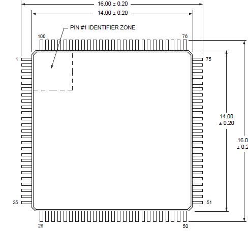
Pinout

  Connection Diagram


Specifications

Parameter Symbol Min Max Unit
Storage Temperature Tstg 65 150
Supply Voltage with Respect to Ground VDD 0.5 7.0 V
VDD5 Supply Voltage with Respect to Ground
(OR2TxxA)
VDD5 VDD 7.0 V
Input Signal with Respect to Ground
OR2TxxA only
- 0.5 VDD + 0.3
VDD5 + 0.3
V
Signal Applied to High-impedance Output
OR2TxxA only
- 0.5 VDD + 0.3
VDD5 + 0.3
V
Maximum Soldering Temperature - - 260  


Description

`The FPGA OR2C04A's functionality is determined by internal configuration RAM. The FPGA's internal   initialization/configuration circuitry loads the configuration data at powerup or under system control. The RAM OR2C04A is loaded by using one of several configuration modes. The configuration data resides externally in an EEPROM, EPROM, or ROM on the circuit board, or any other storage media. Serial ROMs provide a simple, low pin count method for configuring FPGAs OR2C04A, while the peripheral and JTAG configuration modes allow for easy, in-system programming (ISP).


Customers Who Bought This Item Also Bought

Margin,quality,low-cost products with low minimum orders. Secure your online payments with SeekIC Buyer Protection.
Tapes, Adhesives
803
Isolators
Power Supplies - External/Internal (Off-Board)
Circuit Protection
Resistors
Undefined Category
View more