Features: ` High-performance, cost-effective, 0.35 m (OR3C) and 0.3 m (OR3T) 4-level metal technology, (4- or 5-input look-up table delay of 1.1 ns with -7 speed grade in 0.3 m).
`Same basic architecture as lower-voltage, advanced process technology Series 3 architectures. (See ORCA Series 3L FPGA documentation.)
` Up to 186,000 usable gates.
` Up to 452 user I/Os. (OR3Txxx I/Os are 5 V tolerant to allow interconnection to both 3.3 V and 5 V devices, selectable on a per-pin basis.)
` Pin selectable I/O clamping diodes provide 5 V or 3.3 V PCI compliance and 5 V tolerance on OR3Txxx devices.
` Twin-quad programmable function unit (PFU) architecture with eight 16-bit look-up tables (LUTs) per PFU, organized in two nibbles for use in nibble- or byte-wide functions. Allows for mixed arithmetic and logic functions in a single PFU.
` Nine user registers per PFU, one following each LUT, plus one extra. All have programmable clock enable and local set/reset, plus a global set/reset that can be disabled per PFU.
` Flexible input structure (FINS) of the PFUs provides a routability enhancement for LUTs with shared inputs and the logic flexibility of LUTs with independent inputs.
` Fast-carry logic and routing to adjacent PFUs for nibble-, byte-wide, or longer arithmetic functions, with the option to register the PFU carry-out.
` Softwired LUTs (SWL) allow fast cascading of up to three levels of LUT logic in a single PFU for up to 40% speed improvement.
` Supplemental logic and interconnect cell (SLIC) provides 3-statable buffers, up to 10-bit decoder, and PAL*-like AND-OR with optional INVERT in each programmable logic cell (PLC), with over 50% speed improvement typical.
` Abundant hierarchical routing resources based on routing two data nibbles and two control lines per set provide for faster place and route implementations and less routing delay.
` TTL or CMOS input levels programmable per pin for the OR3Cxx (5.0 V) devices.
` Individually programmable drive capability: 12 mA sink/6 mA source or 6 mA sink/3 mA source.
` Built-in boundary scan (IEEE †1149.1 JTAG) and TS_ALL testability function to 3-state all I/O pins.
` Enhanced system clock routing for low skew, high-speed clocks originating on-chip or at any I/O.
` Up to four ExpressCLK inputs allow extremely fast clocking
of signals on- and off-chip plus access to internal general clock routing.
` StopCLK feature to glitchlessly stop/start ExpressCLKs independently by user command.
` Programmable I/O (PIO) has:
- Fast-capture input latch and input flip-flop (FF) latch for reduced input setup time and zero hold time.
- Capability to (de)multiplex I/O signals.
- Fast access to SLIC for decodes and PAL-like functions.
- Output FF and two-signal function generator to reduce CLK to output propagation delay.
- Fast open-drain dive capability
- Capability to register 3-state enable signal.
n Baseline FPGA family used in Series 3+ FPSCs (field programmable system chips) which combine FPGA logic and standard cell logic on one device.
* PAL is a trademark of Advanced Micro Devices, Inc. †IEEE is a registered trademark of The Institute of Electrical and Electronics Engineers, Inc.Application·The applications discussed below are only a small sampling of the possible uses for the PCM. Check the Lucent Technologies ORCA FPGA Internet website (listed at the end of this data sheet) for additional application notes.Pinout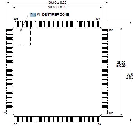 Specifications
| Parameter |
Symbol |
Min |
Max |
Unit |
| Storage Temperature |
Tstg |
65 |
150 |
|
| Supply Voltage with Respect to Ground |
VDD |
0.5 |
7.0 |
V |
| Input Signal with Respect to Ground |
- |
0.5 |
VDD + 0.3 |
V |
| Signal Applied to High-impedance Output |
- |
0.5 |
VDD + 0.3 |
V |
| Maximum Package Body Temperature |
- |
- |
220 |
|
DescriptionThe OR3C55 FPGAs are a new generation of SRAM-based FPGAs built on the successful OR2C/ TxxA FPGA Series from Lucent Technologies Microelectronics Group, with enhancements and innovations geared toward today's high-speed designs and tomorrow's systems on a single chip. Designed from the start to be synthesis friendly and to reduce place and route times while maintaining the complete routability of the ORCA 2C/2T devices, OR3C55 more than doubles the logic available in each logic block and incorporates system- level features that can further reduce logic requirements and increase system speed. OR3C55 devices contain many new patented enhancements and are offered in a variety of packages, speed grades, and temperature ranges.
The OR3C55FPGAs consist of three basic elements: programmable logic cells (PLCs), programmable input/output cells (PICs), and system-level features.
An array of PLCs of OR3C55 is surrounded by PICs. Each PLC contains a programmable function unit (PFU), a supplemental logic and interconnect cell (SLIC), local routing resources, and configuration RAM. Most of the FPGA logic is performed in the PFU, but decoders, PAL-like functions, and 3-state buffering can be performed in the SLIC. The PICs of OR3C55 provide device inputs and outputs and can be used to register signals and to perform input demultiplexing, output multiplexing, and other functions on two output signals. Some of the system- level functions include the new microprocessor interface (MPI) and the programmable clock manager (PCM).
PLC Logic Each PFU of OR3C55 within a PLC contains eight 4-input (16-bit) look-up tables (LUTs), eight latches/flip-flops (FFs), and one additional flip-flop that may be used independently or with arithmetic functions.
The PFU of OR3C55 is organized in a twin-quad fashion: two sets of four LUTs and FFs that can be controlled independently.
LUTs of OR3C55 may also be combined for use in arithmetic functions using fast-carry chain logic in either 4-bit or 8-bit modes. The carry-out of either mode may be registered in the ninth FF for pipelining. Each PFU may also be configured as a synchronous 32 x 4 single- or dual-port RAM or ROM. The FFs (or latches) may obtain input from LUT outputs or directly from invertible PFU inputs, or OR3C55 can be tied high or tied low. The FFs also have programmable clock polarity, clock enables, and local set/reset.
The SLIC of OR3C55 is connected to PLC routing resources and to the outputs of the PFU. It contains 3-state, bidirectional buffers and logic to perform up to a 10-bit AND function for decoding, or an AND-OR with optional INVERT (AOI) to perform PAL-like functions. The 3-state drivers of OR3C55 in the SLIC and their direct connections to the PFU outputs make fast, true 3-state buses possible within the FPGA, reducing required routing and allowing for realworld system performance.

 OR3C55 Data Sheet


