P1817B

Features: `FCC approved method of EMI attenuation.`Generates a low EMI spread spectrum clock of the input frequency.`Optimized for frequency range from:o P1817A 20 to 30MHz. Operationo P1817B 10 to 20MHz Operation`Internal loop filter minimizes external components and board space.`Two selectable...

product image

P1817B Picture
SeekIC No. : 004439052 Detail

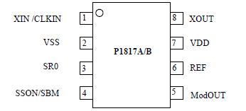
P1817B: Features: `FCC approved method of EMI attenuation.`Generates a low EMI spread spectrum clock of the input frequency.`Optimized for frequency range from:o P1817A 20 to 30MHz. Operationo P1817B 10 t...

floor Price/Ceiling Price

Part Number:
P1817B
Supply Ability:
5000

Price Break

  • Qty
  • 1~5000
  • Unit Price
  • Negotiable
  • Processing time
  • 15 Days
Total Cost: $ 0.00

SeekIC Buyer Protection PLUS - newly updated for 2013!

  • Escrow Protection.
  • Guaranteed refunds.
  • Secure payments.
  • Learn more >>

Month Sales

268 Transactions

Rating

evaluate  (4.8 stars)

Upload time: 2024/4/28

Payment Methods

All payment methods are secure and covered by SeekIC Buyer Protection PLUS.

Notice: When you place an order, your payment is made to SeekIC and not to your seller. SeekIC only pays the seller after confirming you have received your order. We will also never share your payment details with your seller.
Product Details

Description


Features:

`FCC approved method of EMI attenuation.
`Generates a low EMI spread spectrum clock of the input frequency.
`Optimized for frequency range from:
o P1817A 20 to 30MHz. Operation
o P1817B 10 to 20MHz Operation
`Internal loop filter minimizes external components and board space.
`Two selectable spread ranges.
`Low inherent cycle-to-cycle jitter.
`3.3V or 5V operating voltage range.
`TTL or CMOS compatible outputs.
`Ultra-low power CMOS design.
`3.17mA @3.3V, 10MHz | 6.20mA@5.0V, 10MHz
`4.28mA @3.3V, 14MHz | 7.50mA @5.0V, 14MHz
`5.50mA @3.3V, 20MHz | 9.50mA @5.0V, 20MHz
`Supports notebook VGA and other LCD timing controller applications.
`SSON pin for Spread Spectrum On/Off and Standby Mode controls.
`Available in 8-pin SOIC and TSSOP


Application

The P1817 is targeted towards notebook VGA chip and other displays using an LVDS interface, PC peripheral devices, and embedded systems.


Pinout

  Connection Diagram


Specifications

Symbol
Parameter
Rating
Unit
VDD,VIN
Voltage on any pin with respect to GND
-0.5 to + 7.0
V
TSTG
Storage temperature
-65 to +125
°C
TA
Operating temperature
0 to 70
°C
Note: These are stress ratings only and functional operation is not implied. Exposure to absolute maximum ratings for extended periods may affect device reliability.


Description

The P1817 is a versatile spread spectrum frequency modulator designed specifically for input clock frequencies.The P1817 reduces electromagnetic interference (EMI) at the clock source, allowing system wide reduction of EMI of down stream clock and data dependent signals. The P1817 allows significant system cost savings by reducing the number of circuit board layers ferrite beads, shielding and other passive components that are traditionally required to pass EMI regulations.

The P1817 modulates the output of a single PLL in order to "spread" the bandwidth of a synthesized clock, and more importantly, decreases the peak amplitudes of its harmonics. This results in significantly lower system EMI compared to the typical narrow band signal produced by oscillators and most frequency generators. Lowering EMI by increasing a signal's bandwidth is called 'spread spectrum clock generation'.

The P1817 uses the most efficient and optimized modulation profile approved by the FCC and is implemented in a proprietary all digital method.


Customers Who Bought This Item Also Bought

Margin,quality,low-cost products with low minimum orders. Secure your online payments with SeekIC Buyer Protection.
Line Protection, Backups
Hardware, Fasteners, Accessories
Optoelectronics
Semiconductor Modules
Fans, Thermal Management
View more