P89V51RD2FBC

PinoutDescriptionThe P89V51RD2FBC is a kind of 80C51 microcontroller with 64 kB Flash and 1024 bytes of data RAM.A key feature of the P89V51RD2BN is its X2 mode option. The design engineer can choose to run the application with the conventional 80C51 clock rate (12 clocks per machine cycle) or sel...

product image

P89V51RD2FBC Picture
SeekIC No. : 004453776 Detail

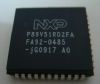
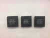
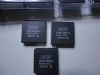
P89V51RD2FBC: PinoutDescriptionThe P89V51RD2FBC is a kind of 80C51 microcontroller with 64 kB Flash and 1024 bytes of data RAM.A key feature of the P89V51RD2BN is its X2 mode option. The design engineer can choos...

floor Price/Ceiling Price

Part Number:
P89V51RD2FBC
Supply Ability:
5000

Price Break

  • Qty
  • 1~5000
  • Unit Price
  • Negotiable
  • Processing time
  • 15 Days
Total Cost: $ 0.00

SeekIC Buyer Protection PLUS - newly updated for 2013!

  • Escrow Protection.
  • Guaranteed refunds.
  • Secure payments.
  • Learn more >>

Month Sales

268 Transactions

Rating

evaluate  (4.8 stars)

Upload time: 2024/4/29

Payment Methods

All payment methods are secure and covered by SeekIC Buyer Protection PLUS.

Notice: When you place an order, your payment is made to SeekIC and not to your seller. SeekIC only pays the seller after confirming you have received your order. We will also never share your payment details with your seller.
Product Details

Description


Pinout

  Connection Diagram


Description

The P89V51RD2FBC is a kind of 80C51 microcontroller with 64 kB Flash and 1024 bytes of data RAM.A key feature of the P89V51RD2BN is its X2 mode option. The design engineer can choose to run the application with the conventional 80C51 clock rate (12 clocks per machine cycle) or select the X2 mode (6 clocks per machine cycle) to achieve twice the throughput at the same clock frequency. Another way to benefit from this feature is to keep the same performance by reducing the clock frequency by half, thus dramatically reducing the EMI.

Features of the P89V51RD2FBC are:(1) 80C51 central processing unit;(2) 5 V operating voltage from 0 to 40 MHz;(3) 64 kB of on-chip Flash program memory with ISP (In-System Programming) and IAP (In-Application Programming);(4) it supports 12-clock (default) or 6-clock mode selection via software or ISP;(5) SPI (Serial Peripheral Interface) and enhanced UART;(6) PCA (programmable counter array) with PWM and capture/compare functions;(7) four 8-bit I/O ports with three high-current Port 1 pins (16 mA each);(8) three 16-bit timers/counters;(9) programmable watchdog timer (WDT);(10) eight interrupt sources with four priority levels.

The absolute maximum ratings of the P89V51RD2FBC can be summarized as:(1): operating bias ambient temperature(Tamb(bias)) is -55°C to +125°C;(2): storage temperature range(Tstg) is -65°C to +150 °C;(3): voltage on EA pin to VSS(VEA) is -0.5 V min and 14 V max;(4): DC voltage on any pin to ground potential(Vn) is -0.5 V to VDD + 0.5 V; (5): transient voltage (<20 ns) on any other pin to VSS (Vit) is -1.0 V min and VDD + 1.0 V max.


Customers Who Bought This Item Also Bought

Margin,quality,low-cost products with low minimum orders. Secure your online payments with SeekIC Buyer Protection.
Soldering, Desoldering, Rework Products
Connectors, Interconnects
Test Equipment
Audio Products
Semiconductor Modules
Boxes, Enclosures, Racks
View more