PDI1284P11

Features: · Asynchronous operation· 8-Bit transceivers· 6 additional buffer/driver lines peripheral to cable· 5 additional control lines from cable· 5V tolerant· ESD protection exceeds 2000V per MIL STD 883 Method 3015 and 200V per Machine Model· Latch up protection exceeds 500 mA per JEDEC Std 19...

product image

PDI1284P11 Picture
SeekIC No. : 004457399 Detail

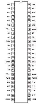
PDI1284P11: Features: · Asynchronous operation· 8-Bit transceivers· 6 additional buffer/driver lines peripheral to cable· 5 additional control lines from cable· 5V tolerant· ESD protection exceeds 2000V per MIL...

floor Price/Ceiling Price

Part Number:
PDI1284P11
Supply Ability:
5000

Price Break

  • Qty
  • 1~5000
  • Unit Price
  • Negotiable
  • Processing time
  • 15 Days
Total Cost: $ 0.00

SeekIC Buyer Protection PLUS - newly updated for 2013!

  • Escrow Protection.
  • Guaranteed refunds.
  • Secure payments.
  • Learn more >>

Month Sales

268 Transactions

Rating

evaluate  (4.8 stars)

Upload time: 2024/4/28

Payment Methods

All payment methods are secure and covered by SeekIC Buyer Protection PLUS.

Notice: When you place an order, your payment is made to SeekIC and not to your seller. SeekIC only pays the seller after confirming you have received your order. We will also never share your payment details with your seller.
Product Details

Description


Features:

· Asynchronous operation
· 8-Bit transceivers
· 6 additional buffer/driver lines peripheral to cable
· 5 additional control lines from cable
· 5V tolerant
· ESD protection exceeds 2000V per MIL STD 883 Method 3015 and 200V per Machine Model
· Latch up protection exceeds 500 mA per JEDEC Std 19
· Input Hysteresis
· Low Noise Operation
· IEEE 1284 Compliant Level 1 & 2
· Overvoltage Protection on B/Y side for OFF-state
· A side 3-State option
· B side active or resistive pull up option
· Cable side VCC for 5V or 3V operation


Pinout

  Connection Diagram


Specifications

SYMBOL
PARAMETER
CONDITIONS
RATING
UNIT
ESD Immunity, per Mil Std 883C method 3015
±1
kV
VCC
DC supply voltage
0.5 to +4.6
V
VCCB
DC cable supply voltage
0.5 to +6.5
V
IIK
DC input diode current
VI < 0
±20
mA
IOK
DC output diode current
VO < 0
±50
mA
VIN
DC input voltage3
0.5 to +5.5
V
VOUT B/Y
DC output voltage on B/Y side3
0.5 to +5.5
V
VOUT B/Y
Transient output voltage on B/Y side4
40ns transient
2 to +7
V
VOUT A
DC output voltage on A side
0.5 to VCC +0.5
V
IO
DC output current
Outputs in High or Low state
±50
mA
Tstg
Storage temperature range
60 to +150
ICC /IGND
Continuous current through VCC or GND
±200
mA


NOTES:
1. Stresses beyond those listed may cause permanent damage to the device. These are stress ratings only and functional operation of the device at these or any other conditions beyond those indicated under "recommended operating conditions" is not implied. Exposure to absolute-maximum-rated conditions for extended periods may affect device reliability.
2. The performance capability of a high-performance integrated circuit in conjunction with its thermal environment can create junction temperatures which are detrimental to reliability. The maximum junction temperature of this integrated circuit should not exceed 150°C.
3. The input and output voltage ratings may be exceeded if the input and output current ratings are observed.
4. VOUT  B/Y (tr) guarantees only that this part will not be damaged by reflections in application so long as the voltage levels remain in the specified range.


Description

The PDI1284P11 parallel interface chip is designed to provide an asynchronous, 8-bit, bi-directional, parallel interface for personal computers. The part includes all 19 signal lines defined by the IEEE1284 interface specification for Byte, Nibble, EPP, and ECP modes. The part is designed for hosts or peripherals operating at 3.3V to interface 3.3V or 5.0V devices.

The PDI1284P11(A/B 1-8) allow data transmission from the A bus to the B bus, or from the B bus to the A bus, depending on the state of the direction pin DIR.

The PDI1284P11 has either totem pole or resistor pull up outputs, depending on the state of the high drive enable pin HD. The A bus has only totem pole style outputs. All inputs are TTL compatible with at least 400mV of input hysteresis at VCC  = 3.3V.


Customers Who Bought This Item Also Bought

Margin,quality,low-cost products with low minimum orders. Secure your online payments with SeekIC Buyer Protection.
RF and RFID
Boxes, Enclosures, Racks
Static Control, ESD, Clean Room Products
Cables, Wires - Management
Motors, Solenoids, Driver Boards/Modules
Potentiometers, Variable Resistors
View more