PEF80902

Features: Features known from the PEB 8090• Single chip solution including U- and S-transceiver• Perfectly suited for the NT1 in the ISDN• Fully automatic activation and deactivation• U-interface (4B3T) conform to ETSI [1] and FTZ [2]: Meets all transmission requirements on...

product image

PEF80902 Picture
SeekIC No. : 004459506 Detail

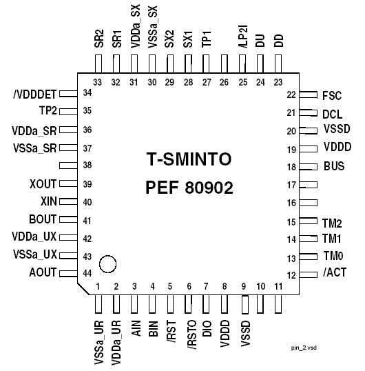
PEF80902: Features: Features known from the PEB 8090• Single chip solution including U- and S-transceiver• Perfectly suited for the NT1 in the ISDN• Fully automatic activation and deactivati...

floor Price/Ceiling Price

Part Number:
PEF80902
Supply Ability:
5000

Price Break

  • Qty
  • 1~5000
  • Unit Price
  • Negotiable
  • Processing time
  • 15 Days
Total Cost: $ 0.00

SeekIC Buyer Protection PLUS - newly updated for 2013!

  • Escrow Protection.
  • Guaranteed refunds.
  • Secure payments.
  • Learn more >>

Month Sales

268 Transactions

Rating

evaluate  (4.8 stars)

Upload time: 2024/4/30

Payment Methods

All payment methods are secure and covered by SeekIC Buyer Protection PLUS.

Notice: When you place an order, your payment is made to SeekIC and not to your seller. SeekIC only pays the seller after confirming you have received your order. We will also never share your payment details with your seller.
Product Details

Description


Features:

Features known from the PEB 8090
• Single chip solution including U- and S-transceiver
• Perfectly suited for the NT1 in the ISDN
• Fully automatic activation and deactivation
• U-interface (4B3T) conform to ETSI [1] and FTZ [2]:
Meets all transmission requirements on all ETSI and FTZ loops with margin
• S/T-interface conform to ETSI [4], ANSI [5] and ITU [6]
Supports point-to-point and bus configurations
Meets and exceeds all transmission requirements
• Optional IOM®-2 interface eases chip testing and evaluation
• Power-on reset and Undervoltage Detection with no external components
• ESD robustness 2kV
• Optional use of transformers with non-negligible resistance corresponding to up to 20Ω on the line sidePin Vref and the according external capacitor removed
• Inputs accept 3.3V and 5V
• I/O (open drain) accepts pull-up to 3.3V1)
• Pin compatible with Q-SMINTO (2nd Generation)
• LEDs indicating Loopback 2 and activation status
• Lowest power consumption due to
Low power CMOS technology (0.35µ)
Newly optimized low power libraries
High output swing on U- and S-line interface leads to minimized power consumption
Single 3.3 Volt power supply
• 185mW (NTC-T: 233mW) power consumption with random data over ETSI Loop 2.
• 15mW typical power consumption in power down (as NTC-T; NTC-Q: 28mW)


Pinout

  Connection Diagram


Specifications

Parameter

Symbol

Limit Values

Unit

Ambient temperature under bias
TA
-40 to 85
°C
Storage temperature
Tstg
65 to 150
°C
Maximum Voltage on VDD
VDD
4.2
V
Maximum Voltage on any pin with respect to
ground
VS
-0.3 to VDD + 3.3
(max. < 5.5)
V
ESD integrity (according EIA/JESD22-A114B (HBM)): 2 kV
Note: Stress above those listed here may cause permanent damage to the device.
Exposure to absolute maximum ratings conditions for extended periods may affect
device reliability.


Customers Who Bought This Item Also Bought

Margin,quality,low-cost products with low minimum orders. Secure your online payments with SeekIC Buyer Protection.
Test Equipment
Isolators
Discrete Semiconductor Products
Integrated Circuits (ICs)
Programmers, Development Systems
Resistors
View more