Features: • Signaling Rates >660 Mbps (330 MHz)
• Single 3.3V Power Supply Design
• Driver:- ±350mV Differential Swing into a 100-Ohm load- Propogation Delay of 1.5ns Typ.- Low Voltage TTL (LVTTL) Inputs are 5V Tolerant- Driver is High Impedance when Disabled or VCC <1.5V
• Receiver:- Accepts ±50mV (min.) Differential Swing with up to 2.0Vground potential difference- Propagation Delay of 3.3ns Typ.- Low Voltage TTL (LVTTL) Outputs- Open, Short, and Terminated Fail Safe
• Industrial Temperature Operating Range: 40°C to 85°C
• Package Options: SOIC, TSSOP, MSOP
• Meets or Exceeds IEEE 1596.3 SCI Standard
• Meets or Exceeds ANSI/TIA/EIA-644 LVDS Standard
• Bus-Terminal ESD exceeds 12kVApplicationApplications include point-to-point and multidrop baseband datatransmission over a controlled impedance media of approximately100 ohms. These include intra-system connections via printedcircuit board traces or cables, hubs and routers for data communications;PBXs, switches, repeaters and base stations for telecommunicationsand other applications such as digital cameras, printersand copiers.
Pinout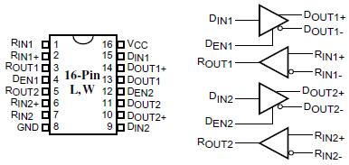
SpecificationsSupply Voltage (VCC) ....................................................0.5V to +4.0V
Driver
Input Voltage (DIN) ....................................... 0.3V to (Vcc + 0.3V)
Output Voltage (DOUT+, DOUT-) ...............................0.3V to +3.9V
Short Circuit Duration (DOUT+, DOUT-) ......................... Continuous
Enable Input Voltage (DEN) ............................ 0.3V to (VCC + 0.3V)
Receiver
Input Voltage (RIN+, RIN-) ........................................ 0.3V to +3.9V)
Output Voltage (ROUT) ................................... 0.3V to (VCC + 0.3V)
Enable Input Voltage (REN*) ........................... 0.3V to (VCC + 0.3V)
Storage Temperature Range .................................. 65°C to +150°C
Lead Temperature Range Soldering (4s) ...............................+260°C
Maximum Junction Temperature ............................................+150°C
ESD Rating ............................................................................... >12kVDescriptionThe PI90LV179, PI90LV180, PI90LV050, and PI90LV051 are differentialline drivers and receivers (transceivers) that are compliant withthe IEEE 1596.3 SCI and ANSI/TIA/EIA-644 LVDS standards. PI90LV179, PI90LV180, PI90LV050, and PI90LV051 use low-voltage differential signaling (LVDS) to achievedata rates in excess of 660 Mbps while being less susceptible to noisethan single-ended transmission.
The PI90LV179, PI90LV180, PI90LV050, and PI90LV051 translate a low-voltage TTL/CMOS input into a lowvoltage(350mV typical) differential output signal. The receiverstranslate a differential 350mV input signal to a 3V CMOS output level.
The driver section of PI90LV179, PI90LV180, PI90LV050, and PI90LV051 can be independently set to a power-down andhigh-impedance output mode with the DEN pin (active HIGH). Thereceiver section is controlled by the REN* pin (active LOW).

 PI90LV051 Data Sheet