Features: • High Density 32 channel T1/E1/J1 framer.
• Software selectable between T1/J1 or E1 operation on a per device basis.
• Supports 8 Mbit/s H-MVIP on the system interface for all T1 or E1 links, a separate 8 Mbit/s H-MVIP system interface for all T1 or E1 CAS channels and a separate 8 Mbit/s H-MVIP system interface for all T1 or E1 CCS and V5.1/V5.2 channels.
• Supports a byte serial Scaleable Bandwidth Interconnect (SBI) bus interface for high density system side device interconnection of up to 32 T1 streams, 32 E1 streams.
• Provides jitter attenuation in the T1 or E1 receive and transmit directions.
• Provides three independent de-jittered T1 or E1 recovered clocks for system timing and redundancy.
• Provides per link diagnostic and line loopbacks.
• Also provides PRBS generators and detectors on each tributary for error testing at DS1, E1 and NxDS0 rates as recommended in ITU-T O.151 and O.152.
• Provides a generic 8-bit microprocessor bus interface for configuration, control and status monitoring. Provides a standard 5 signal P1149.1 JTAG test port for boundary scan board test purposes.
• Low power 1.8V/3.3V CMOS technology. All pins are 5V tolerant.
• 324-pin fine pitch PBGA package (23mm x 23mm). Supports industrial temperature range (-40 oC to 85 oC) operation.
• Line side interface is SBI bus.
• System side interface is either H-MVIP or SBI bus. Each one of 32 T1 receiver sections:
• Frames to DS-1 signals in SF, SLC96 and ESF formats.
• Frames to TTC JT-G.704 multiframe formatted J1 signals. Supports the alternate CRC-6 calculation for Japanese applications.
• Provides Red, Yellow, and AIS alarm integration.
• Supports RAI-CI and AIS-CI alarm detection and generation.
• Provides ESF bit-oriented code detection and an HDLC/LAPD interface for terminating the ESF facility data link.
• Provides Inband Loopback Code generation and detection.
• Indicates signaling state change, and two superframes of signaling debounce on a per-DS0 basis.
• Provides an HDLC interface with 128 bytes of buffering for terminating the facility data link.
• Provides performance monitoring counters sufficiently large as to allow performance monitor counter polling at a minimum rate of once per second. Optionally, updates the performance monitoring counters and interrupts the microprocessor once per second, timed to the receive line.
• Provides an optional elastic store, which may be used to time the ingress streams to a common clock and frame alignment in support of a H-MVIP interface.
• Provides DS-1 robbed bit signaling extraction and insertion, with optional data inversion, programmable idle code substitution, digital milliwatt code substitution, bit fixing, and two superframes of signaling debounce on a perchannel basis.
• A pseudo-random sequence user selectable from 27 1, 211 1, 215 1 or 220 1, may be detected in the T1 stream in either the ingress or egress directions. The detector counts pattern errors using a 16-bit non-saturating PRBS error counter. The pseudo-random sequence can be the entire T1 or any combination of DS0s within a framed T1.
• Frames in the presence of and detects the "Japanese Yellow" alarm.
• Supports the alternate CRC-6 calculation for Japanese applications.
• Provides external access for up to three de-jittered recovered T1 clocks. Each one of 32 E1 receiver sections:
• Frames to ITU-T G.704 basic and CRC-4 multiframe formatted E1 signals. The framing procedures are consistent ITU-T G.706 specifications.
• Provides an HDLC interface with 128 bytes of buffering for terminating the national use bit data link.
• Extracts 4-bit codewords from the E1 national use bits as specified in ETS 300 233.
• V5.2 link indication signal detection.
• Provides performance monitoring counters sufficiently large as to allow performance monitor counter polling at a minimum rate of once per second. Optionally, updates the performance monitoring counters and interrupts the microprocessor once per second, timed to the receive line.
• Provides a two-frame elastic store buffer for backplane rate adaptation that performs controlled slips and indicates slip occurrence and direction.
• Frames to the E1 signaling multiframe alignment when enabled and extracts channel associated signaling. Alternatively, a common channel signaling data link may be extracted from timeslot 16.
• Can be programmed to generate an interrupt on change of signaling state.
• Provides trunk conditioning which forces programmable trouble code substitution and signaling conditioning on all channels or on selected channels.
• A pseudo-random sequence user selectable from 27 1, 211 1, 215 1 or 220 1, may be detected in the E1 stream in either the ingress or egress directions. The detector counts pattern errors using a 16-bit non-saturating PRBS error counter. The pseudo random sequence can be the entire E1 or any combination of timeslots within the framed E1.
• Provides external access for up to three de-jittered recovered E1 clocks. Each one of 32 T1 transmitter sections:
• May be timed to its associated receive clock (loop timing) or may derive its timing from a common egress clock or a common transmit clock; the transmit line clock may be synthesized from an N*8 kHz reference.
• Provides minimum ones density through Bell (bit 7), GTE or "jammed bit 8" zero code suppression on a per-DS0 basis. Provides a 128 byte buffer to allow insertion of the facility data link using the host interface.
• Supports transmission of the alarm indication signal (AIS) or the Yellow alarm signal in SF, SLC96 and ESF formats.
• Provides transparency for the F-bit to support SLC96 data link insertion.
• Autonomously transmits an ESF Performance Report Message each second.
• Provides a digital phase locked loop for generation of a low jitter transmit clock.
• Provides a FIFO buffer for jitter attenuation and rate conversion in the transmitter.
• Supports the alternate ESF CRC-6 calculation for Japanese applications.
• A pseudo-random sequence user selectable from 27 1, 211 1, 215 1 or 220 1, may be inserted into the T1 stream in either the ingress or egress directions. The pseudo-random sequence can be inserted into the entire T1 or any combination of DS0s within the framed T1.Each one of 32 E1 transmitter sections:
• Provides a FIFO buffer for jitter attenuation and rate conversion in the transmit path.
• Transmits G.704 basic and CRC-4 multiframe formatted E1.
• Supports unframed mode and framing bit, CRC, or data link by-pass.
• Provides signaling insertion, programmable idle code substitution, digital milliwatt code substitution, and data inversion on a per channel basis.
• Provides trunk conditioning which forces programmable trouble code substitution and signaling conditioning on all channels or on selected channels.
• Provides a digital phase locked loop for generation of a low jitter transmit clock.
• A pseudo-random sequence user selectable from 27 1, 211 1, 215 1 or 220 1, may be inserted into the E1 stream in either the ingress or egress directions. The pseudo-random sequence can be inserted into the entire E1 or any combination of timeslots within the framed E1.
• Optionally inserts a datalink in the E1 national use bits.
• Supports 4-bit codeword insertion in the E1 national use bits as specified in ETS 300 233
• Supports transmission of the alarm indication signal (AIS) and the remote alarm indication (RAI) signal. Six full featured T1/E1 Pattern Generators and Detectors:
• Each generator and detector pair may be associated with any one of the 32 T1s or E1s.
• Any sub-set of DS0s within a tributary may be selected.
• Provides programmable pseudo-random test sequence generation (up to 232- 1 bit length sequences conforming to ITU-T O.151 standards) or any repeating pattern up to 32 bits. Diagnostic abilities include single bit error insertion or error insertion at bit error rates ranging from 10-1 to 10-7. Synchronous System Interfaces:
• Provides eight 8 Mbit/s H-MVIP data interfaces for synchronous access to all the DS0s of all 32 T1 links or all timeslots of all 32 E1s.
• Provides 8 8 Mbit/s H-MVIP interfaces for synchronous access to all channel associated signaling (CAS) bits for all T1 DS0s or E1 timeslots. The CAS bits occupy one nibble of every byte on the H-MVIP interfaces and are repeated over the entire T1 or E1 multi-frame.
• Provides three 8 Mbit/s H-MVIP interfaces for common channel signaling (CCS) channels as well as V5.1 and V5.2 channels. In T1 mode DS0 24 is available through this interface. In E1 mode timeslots 15, 16 and 31 are available through this interface. Optionally, timeslot 0 may be presented instead of timeslot 15.
• All links accessed via the H-MVIP interface will be synchronously timed to the common H-MVIP clock and frame alignment signals, CMV8MCLK, CMVFP, CMVFPC.
• H-MVIP access for Channel Associated Signaling is available with the Scaleable Bandwidth Interconnect bus as an optional replacement for CAS access over the SBI bus as well as with the H-MVIP data interface. Common Channel Signaling H-MVIP access is available with the SBI bus, serial PCM and H-MVIP data interfaces.
• Alarm status, T1 F-bit and inband signaling control is available using otherwise unused bit positions.
• Compatible with H-MVIP PCM backplanes supporting 8.192 Mbit/s. Scaleable Bandwidth Interconnect (SBI) Bus:
• Provides a high density byte serial interconnect for all TE-32 links. Utilizes an Add/Drop configuration to asynchronously multiplex up to 32 T1s or 32 E1s with multiple payload or link layer processors.
• External devices can access framed T1s and framed E1s over this interface.
• Framed T1 access can be selected on a per T1 basis. Framed E1 access can be selected on a per E1 basis.
• At the system interface, synchronous access for T1 DS0 channels or E1 timeslots is supported in a locked format mode. Selectable on a per tributary basis.
• At the system interface, channel associated signaling bits for channelized T1 and E1 are explicitly identified across the bus.
• Transmit timing is mastered either by the TE-32 or a layer 2 device connecting to the system interface SBI bus. Timing mastership is selectable on a per tributary basis, where a tributary is either an individual T1, E1.
• The line side SBI bus provides a time switch capability in support of redundancy.
• The system side SBI operates at either 19.44 MHz or 77.76 MHz. The line side SBI operates at 19.44 MHz.
Application• Multiservice Switches
• Voice Gateways
• Wireless Base Station Controllers
• Edge Routers
• Multiservice Add-Drop Multiplexers
• Digital Access Cross-Connect SystemsSpecifications
| Parameter |
Symbol |
Value |
Units |
| Ambient Temperature under Bias |
|
-40 to +85 |
°C |
| Storage Temperature |
TST |
-40 to +125 |
°C |
| Supply Voltage |
VDD1.8 |
-0.3 to + 3.6 |
VDC |
| Supply Voltage |
VDD3.3 |
-0.3 to + 6.0 |
VDC |
| Voltage on Any Pin |
VIN |
-0.3 to 6.0 |
VDC |
| Static Discharge Voltage |
|
±1000 |
V |
| Latch-Up Current |
|
±100 |
mA |
| DC Input Current |
IIN |
±20 |
mA |
| Lead Temperature |
|
+230 |
°C |
| Junction Temperature |
TJ |
+150 |
°C |
Notes on Power Supplies:
1. VDD3.3 should power up before VDD1.8.
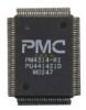
2. VDD3.3 should not be allowed to drop below the VDD1.8 voltage level except when VDD1.8 is not powered.DescriptionThe PM4332 High Density 32 Channel T1/E1 Framer is a feature-rich device for use in any application requiring high density framing of T1/J1 and E1 links.
Each of the T1 and E1 framers and transmitters is independently software configurable, PM4332 allowing timing master and feature selection without changes to external wiring. However, mixed framing modes are not supported. The framers PM4332 nmust be all configured for either T1 or E1 framing.

 PM4332 Data Sheet