Features: • High-performance RISC CPU
• Specially tested
- 16MHz @ 3V
• Only 35 single word instructions to learn
• All single cycle instructions except for program branches which are two cycle
• Operating speed: DC - 16 MHz clock input DC - 250 ns instruction cycle
• 4K x 14 words of Program Memory, 192 x 8 bytes of Data Memory (RAM)
• Interrupt capability
• Eight level deep hardware stack
• Direct, indirect and relative addressing modes
• Power-on Reset (POR)
• Power-up Timer (PWRT) and Oscillator Start-up Timer (OST)
• Watchdog Timer (WDT) with its own on-chip RC oscillator for reliable operation
• Programmable code-protection
• Power saving SLEEP mode
• Selectable oscillator options
• Low-power, high-speed CMOS EPROM technology
• Wide operating voltage range: 2.5V to 5.5V
• High Sink/Source Current 25/25 mA
• Commercial, Industrial and Automotive temperature ranges
• Low-power consumption:
- < 5 mA @ 5V, 4 MHz
- 23 A typical @ 3V, 32 kHz
- < 3 A typical standby current Pin Diagram:
Peripheral Features:
• Timer0: 8-bit timer/counter with 8-bit prescaler
• Timer1: 16-bit timer/counter with prescaler can be incremented during sleep via external crystal/clock
• Timer2: 8-bit timer/counter with 8-bit period register, prescaler and postscaler
• Capture, Compare, PWM module(s)
- Capture is 16 bit, max. resolution is 15.6 ns
- Compare is 16 bit, max. resolution is 250 ns
- PWM max. resolution is 10 bit
• 8-bit multichannel analog-to-digital converter
• Synchronous Serial Port (SSP) with SPITM and I2CTM
• Universal Synchronous Asynchronous Receiver Transmitter (USART/SCI)
• Parallel Slave Port (PSP), 8-bits wide, with external RD, WR and CS controls
• Brown-out detection circuitry for Brown-out Reset (BOR) Pin Diagrams
Pinout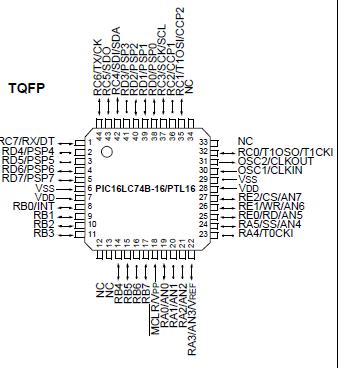 Specifications
Ambient temperature under bias............................................................-55°C to +125°C
Storage temperature ............................................................................ -65°C to +150°C
Voltage on any pin with respect to VSS (except VDD, MCLR, and RA4)..-0.3V to (VDD + 0.3V)
Voltage on VDD with respect to VSS ........................................................... -0.3V to +7.5V
Voltage on MCLR with respect to VSS (Note 2)........................................... 0V to +13.25V
Voltage on RA4 with respect to Vss .............................................................. 0V to +8.5V
Total power dissipation (Note 1)..............................................................................1.0W
Maximum current out of VSS pin ...........................................................................300 mA
Maximum current into VDD pin .............................................................................250 mA
Input clamp current, IIK (VI < 0 or VI >VDD)....................................................... ±20 mA
Output clamp current, IOK (VO < 0 or VO >VDD) ................................................ ±20 mA
Maximum output current sunk by any I/O pin........................................................25 mA
Maximum output current sourced by any I/O pin ...................................................25 mA
Maximum current sunk by PORTA, PORTB, and PORTE (combined)........................200 mA
Maximum current sourced by PORTA, PORTB, and PORTE (combined) ..................200 mA
Maximum current sunk by PORTC and PORTD (combined) ....................................200 mA
Maximum current sourced by PORTC and PORTD (combined) ...............................200 mA
Note 1: Power dissipation is calculated as follows: Pdis = VDD x {IDD - IOH} + {(VDD-VOH) x IOH} + (VOl x IOL)
Note 2: Voltage spikes below VSS at the MCLR/VPP pin, inducing currents greater than 80 mA, may cause latch-up.
Thus, a series resistor of 50-100 should be used when applying a "low" level to the MCLR/VPP pin rather than pulling this pin directly to VSS.
DescriptionThis data sheet covers the PIC16LC74B-16/PTL16 device. The functional characteristics of this device are identical to the PIC16LC74B. For electrical specifications, see the electrical specifications contained within this document. For all other information about this device, see the PIC16C63A/65B/73B/74B data sheet (DS30605).

 PTL16LC74B-16 Data Sheet