PXB42221E

Features: • Full duplex ATM Packetizer/Depacketizer for 8 E1/T1 highways• Configurable to T1 or E1 mode via external pin• 8 T1/E1 ports configurable independently to ATM or AAL Mode• ATM Mode (PXB 4219/4220/4221): ATM cell mapping into PDH according to ITUT G.804 [26] B-ISD...

product image

PXB42221E Picture
SeekIC No. : 004467441 Detail

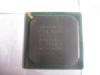
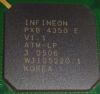
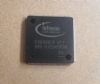
PXB42221E: Features: • Full duplex ATM Packetizer/Depacketizer for 8 E1/T1 highways• Configurable to T1 or E1 mode via external pin• 8 T1/E1 ports configurable independently to ATM or AAL Mod...

floor Price/Ceiling Price

Part Number:
PXB42221E
Supply Ability:
5000

Price Break

  • Qty
  • 1~5000
  • Unit Price
  • Negotiable
  • Processing time
  • 15 Days
Total Cost: $ 0.00

SeekIC Buyer Protection PLUS - newly updated for 2013!

  • Escrow Protection.
  • Guaranteed refunds.
  • Secure payments.
  • Learn more >>

Month Sales

268 Transactions

Rating

evaluate  (4.8 stars)

Upload time: 2024/4/26

Payment Methods

All payment methods are secure and covered by SeekIC Buyer Protection PLUS.

Notice: When you place an order, your payment is made to SeekIC and not to your seller. SeekIC only pays the seller after confirming you have received your order. We will also never share your payment details with your seller.
Product Details

Description


Features:

• Full duplex ATM Packetizer/Depacketizer for 8 E1/T1 highways
• Configurable to T1 or E1 mode via external pin
• 8 T1/E1 ports configurable independently to ATM or AAL Mode
• ATM Mode (PXB 4219/4220/4221):
ATM cell mapping into PDH according to ITUT G.804 [26]
B-ISDN User-Network interface - Physical Layer according to ITU-T I.432 [32]
B-ISDN User-Network interface - Physical Layer operation at 1544 KBit/s and 2048 KBit/s according to ITU-T I.432.3 [34]
• AAL Mode (PXB 4220/4221):
AAL1 according to ITU-T I.363.1 [31] or transparent without any adaptation layer overhead (AAL0)
T1/E1 unstructured service according to ATM Forum af-vtoa-0078.000 [10] section 3
Structured T1/E1 N x 64 kbit/s service according to [10] section 2 with M channels of N x 64 kbit/s (M,N = 1to 24 for T1) (M,N = 1to 32 for E1)
Channel Associated Signalling (CAS) support according to [10]
Echo Canceller Mode
Partially filled cells with programmable filling thresholds
Selectable Sequence Count Algorithm:
Robust/Fast according to ITU-T I.363.1 [30]
According to ETSI (prl-ETS 300353 annex D) [17]
Fast: Saves 6 ms during reassembly for 1 x 64 kbit/s connection
AAL0 option: 48 Bytes user payload per ATM Cell, without AAL overhead
Reassembly buffer can compensate up to +/- 4 ms Cell Delay Variation (CDV)
Statistics counters per channel for lost/misinserted/errored cells etc.
Internal clock recovery circuit using Synchronous Residual Time Stamp (SRTS, for fully filled cells only) or Adaptive Clock Method (ACM) for unstructured CES ports.For SRTS a patent fee needs to be paid. Optionally, it's possible to order the PXB 4221 device, which comes without SRTS clock recovery.
Trunk freezing and conditioning according to Bellcore TR-NWT-000170 [14]
• IMA interface:
Programmable threshold between read and write pointer of Mapping Buffer
Output Signal for buffer threshold crossing
Output Signal for discarded cell
Output pins for port number indication
• 8 generic framer interfaces with integrated transmit clock selector supporting
Synchronous Mode (SYM) for E1
Generic Interface Mode (GIM)
FALC Mode (FAM): Glue-less interface for Infineon's Framer and Line Interface Components (FALC)
Echo Canceller Mode (EC): ATM cells are duplicated internally and transmitted via two framer ports
• UTOPIA industry standard interface:
Level 2 in slave mode; 8 data, 5 address lines
Level 1 in master/slave mode
UTOPIA clock up to 38.88 MHz
• 16-bit generic microprocessor interface for control and configuration of the chip runs either in Intel 386EX or Motorola compatible mode
• External synchronous Flow-Through SSRAM 1 x 64k x 33 bit or 1 x 64k x 32 bit required
• Build-in data path loops for test
• Cell insertion/extraction via microprocessor interface
• 3.3 Volt power supply with 5 Volt tolerant inputs
• Typical power dissipation 1 Watt
• P-BGA-256 package
• Temperature range from -40 to +85


Specifications

Parameter Symbol Limit Values Unit
Ambient temperature under bias TA -40 to 85
Junction temperature under bias TJ 0 to 125
Storage temperature Tstg - 65 to 150
Supply voltage VCC - 0.5 to 3.6 V
Input voltage
(at any signal pin with respect to ground)
VI - 0.5 to 5.5 V
Output voltage level
(at any signal pin with respect to ground)
VO - 0.5 to 5.51) V
ESD robustness2)
HBM: 1.5 kW, 100 pF
VESD,HBM 1000 V
1) The maximum high output level is limited to VCC. Due to 5V I/O tolerance output signals might be pulled to 5Vlevel by external pull-up resistors.
2) According to MIL-Std 883D, method 3015.7 and ESD Ass. Standard EOS/ESD-5.1-1993.The RF Pins 20, 21, 26, 29, 32, 33, 34 and 35 are not protected against voltage stress > 300 V (versus VS or GND). The high frequency performance prohibits the use of adequate protective structures


Customers Who Bought This Item Also Bought

Margin,quality,low-cost products with low minimum orders. Secure your online payments with SeekIC Buyer Protection.
Test Equipment
Inductors, Coils, Chokes
Cable Assemblies
RF and RFID
Static Control, ESD, Clean Room Products
Discrete Semiconductor Products
View more