Features: • Adjustable rise and fall times• Low supply current• Capable of driving 30 nF || 400• Digitally selectable 12.5 or 100 kbit/sec data rate• Adjustable output voltages swing• Output overvoltage protected• Short circuit protected• TTL and CMO...
RM3182A: Features: • Adjustable rise and fall times• Low supply current• Capable of driving 30 nF || 400• Digitally selectable 12.5 or 100 kbit/sec data rate• Adjustable output ...
SeekIC Buyer Protection PLUS - newly updated for 2013!
268 Transactions
All payment methods are secure and covered by SeekIC Buyer Protection PLUS.

|
Parameter |
Min |
Max |
Unit |
| Supply Voltage (VCC to VEE) |
- |
_36 |
V |
| VLOGIC Theshold Voltage |
- |
+7 |
V |
| VREF Voltage |
- |
+VCC |
V |
| Logic Input Voltage |
-0.3 |
VLOGIC+0.3 |
V |
| Storage Temperature Range |
-65 |
+150 |
|
| Operating Temperature Range |
-55 |
+125 |
|
| Junction Temperature |
-55 |
+175 |
|
| Lead Soldering Temperature (60 sec.) |
+300 |
The RM3182A is a complete differential line driver IC. When Data A = Data B or Sync or Clock Signal is low, the driver forces the output to a Voltage Null level (0V ± 250 mV).
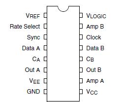
Designed to address the ARINC 429 standard,the RM3182A has output rise and fall times that can be adjusted by the selection of an external capacitor (CA or CB) and an output voltage range adjustable through an externally applied VREF signal. All logic inputs and sync control inputs are TTL/CMOS compatible. The device is constructed on a monolithic IC using a junction-isolated bipolar process.
Sputtered SiCr resistors in the internal bias circuitry provide for stable bias currents and a tighter tolerance of output impedance. The RM3182A is available in 16-lead ceramic sidebrazed DIP.