RM805

Features: • Low voltage positive bias supply• Good linearity• High efficiency• Dual mode operation• Large dynamic range• 28-pin LCC package (10 x 13.97 x 1.7 mm)• Power down controlApplication• PMR (806825 MHz)• TETRA (806825 MHz)• TDMA (...

product image

RM805 Picture
SeekIC No. : 004477953 Detail

RM805: Features: • Low voltage positive bias supply• Good linearity• High efficiency• Dual mode operation• Large dynamic range• 28-pin LCC package (10 x 13.97 x 1.7 mm)&...

floor Price/Ceiling Price

Part Number:
RM805
Supply Ability:
5000

Price Break

  • Qty
  • 1~5000
  • Unit Price
  • Negotiable
  • Processing time
  • 15 Days
Total Cost: $ 0.00

SeekIC Buyer Protection PLUS - newly updated for 2013!

  • Escrow Protection.
  • Guaranteed refunds.
  • Secure payments.
  • Learn more >>

Month Sales

268 Transactions

Rating

evaluate  (4.8 stars)

Upload time: 2024/4/26

Payment Methods

All payment methods are secure and covered by SeekIC Buyer Protection PLUS.

Notice: When you place an order, your payment is made to SeekIC and not to your seller. SeekIC only pays the seller after confirming you have received your order. We will also never share your payment details with your seller.
Product Details

Description


Features:

• Low voltage positive bias supply
• Good linearity
• High efficiency
• Dual mode operation
• Large dynamic range
• 28-pin LCC package (10 x 13.97 x 1.7 mm)
• Power down control


Application

• PMR (806825 MHz)
• TETRA (806825 MHz)
• TDMA (824849 MHz)
• AMPS (824-849 MHz)
• Wireless Local Loop


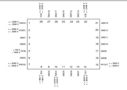
Pinout

  Connection Diagram


Specifications

Parameter Symbol Minimum Nominal Maximum Unit
RF Input Power(2) Pin - 8.0 11.0 dBm
Supply Voltage Vcc - 3.5 6.9(3) Volts
Regulation Voltage Vreg 0.0 2.75 Vcc(4) Volts
Case Operating Temperature Tc -30 +25 +110
Storage Temperature Tstg -55 - +125
(1) No damage assuming only one parameter is set at limit at a time with all other parameters set at or below
nominal value.
(2) Pulsed operation at 25% duty cycle.
(3) When amplifier is biased off (Vreg = 0 V)
(4) Voltage on Vreg pin may not exceed the applied Vcc voltage.


Description

The evaluation board is a platform for testing and interfacing design circuitry. To accommodate the interface testing of the RM805, the evaluation board schematic and assembly diagram are included for preliminary analysis and design. Figure 1 shows the basic schematic of the board for the 806 MHz to 849 MHz range and Figure 2 illustrates the board layout.


Customers Who Bought This Item Also Bought

Margin,quality,low-cost products with low minimum orders. Secure your online payments with SeekIC Buyer Protection.
Sensors, Transducers
Cables, Wires
Static Control, ESD, Clean Room Products
Crystals and Oscillators
Memory Cards, Modules
View more