ROMEO2

Application· 868MHz, 902-928MHz Bands· OOK and FSK Demodulation· Low Current Consumption: 7mA Typ. in Run Mode· Internal or External Strobing· Fast Wake-Up Time (1ms)· -105dBm RF Sensitivity (at 4.8kBd Data Rate)· Fully Integrated VCO· Image Cancelling Mixer· Integrated IF Bandpass Filter at 660kH...

product image

ROMEO2 Picture
SeekIC No. : 004478816 Detail

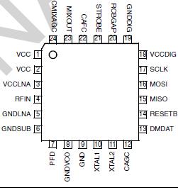
ROMEO2: Application· 868MHz, 902-928MHz Bands· OOK and FSK Demodulation· Low Current Consumption: 7mA Typ. in Run Mode· Internal or External Strobing· Fast Wake-Up Time (1ms)· -105dBm RF Sensitivity (at 4.8...

floor Price/Ceiling Price

Part Number:
ROMEO2
Supply Ability:
5000

Price Break

  • Qty
  • 1~5000
  • Unit Price
  • Negotiable
  • Processing time
  • 15 Days
Total Cost: $ 0.00

SeekIC Buyer Protection PLUS - newly updated for 2013!

  • Escrow Protection.
  • Guaranteed refunds.
  • Secure payments.
  • Learn more >>

Month Sales

268 Transactions

Rating

evaluate  (4.8 stars)

Upload time: 2024/4/27

Payment Methods

All payment methods are secure and covered by SeekIC Buyer Protection PLUS.

Notice: When you place an order, your payment is made to SeekIC and not to your seller. SeekIC only pays the seller after confirming you have received your order. We will also never share your payment details with your seller.
Product Details

Description


Application

· 868MHz, 902-928MHz Bands
· OOK and FSK Demodulation
· Low Current Consumption: 7mA Typ. in Run Mode
· Internal or External Strobing
· Fast Wake-Up Time (1ms)
· -105dBm RF Sensitivity (at 4.8kBd Data Rate)
· Fully Integrated VCO
· Image Cancelling Mixer
· Integrated IF Bandpass Filter at 660kHz
· IF Bandwidth: 500kHz
· ID Byte and Tone Detection
· Data Rate: 1 to 11kBd
· Manchester Coded Data Clock Recovery
· Fully Configurable by SPI Interface
· Few External Components, no RF Adjustment


Pinout

  Connection Diagram


Specifications

Parameter Symbol Value Unit
Supply Voltage VCC
VCCLNA
VGND - 0.3 to 5.5 V
Voltage Allowed on Each Pin   VGND - 0.3
to VCC + 0.3
V
ESD HBM Voltage Capability on Each Pin (note 1)   ±2000 V
ESD MM Voltage Capability on Each Pin (note 2)   ±200 V
Solder Heat Resistance Test (10 s)   260
Storage Temperature Ts -65 to +150
Junction Temperature Tj 150
Notes:
1 Human Body model, AEC-Q100-002 Rev. C.
2 Machine Model, AEC-Q100-003 Rev. E.


Description

The basic functionality of the ROMEO2 receiver may be seen by reference to the accompanying block diagram (see figure 1). ROMEO2 is fully compatible with the TANGO3 transmitter.

The RF section ROMEO2 comprises a mixer with image cancelling, followed by an IF band-pass filter at 660kHz, an AGC controlled gain stage and OOK and FSK demodulators, the desired modulation type being selectable by the SPI interface. The data output from the circuit may either be the data comparator output, or, if Data Manager is enabled, the SPI port.

The local oscillator ROMEO2 is controlled with a PLL referenced to the crystal oscillator. The received channel is defined by the choice of the crystal frequency.

An SPI bus permits programming the modulation type, data rate, UHF frequency, ID word etc., though to accomodate applications where no bus interface is available the circuit defaults at power-on to a standard operating mode.

Depending upon the configuration, the circuit can be either externally strobed by the STROBE input or internally wait-and-sleep cycled to reduce the power consumption. At any time, a high level on STROBE overrides the internal timer output and wakes up ROMEO2. When the circuit is switched into sleep mode its current consumption is approximately 100A. The circuit configuration which has previously been programmed is retained.


Customers Who Bought This Item Also Bought

Margin,quality,low-cost products with low minimum orders. Secure your online payments with SeekIC Buyer Protection.
Hardware, Fasteners, Accessories
Optical Inspection Equipment
Audio Products
Inductors, Coils, Chokes
Crystals and Oscillators
View more