Features: Memory Protection Features`Memory Protection W# pin works in conjunction with Status RegisterBits to protect specified memory areas Status Register Block Protection bits (BP2, BP1, BP0) in status register configure parts of memory as read-onlySoftware Features SPI Bus Compatible Serial...
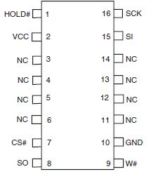
S25FL016A: Features: Memory Protection Features`Memory Protection W# pin works in conjunction with Status RegisterBits to protect specified memory areas Status Register Block Protection bits (BP2, BP1, BP0) ...
SeekIC Buyer Protection PLUS - newly updated for 2013!
268 Transactions
All payment methods are secure and covered by SeekIC Buyer Protection PLUS.
PinoutDescriptionThe S25FL002D0FMAI001 is designed as a 3.0V (2.7V to 3.6V) single power supply fl...
Memory Protection Features
`Memory Protection
W# pin works in conjunction with Status Register
Bits to protect specified memory areas
Status Register Block Protection bits (BP2, BP1, BP0)
in status register configure parts of memory as read-only
Software Features
SPI Bus Compatible Serial Interface

|
Description |
Rating |
| Ambient Storage Temperature | 65°C to +150°C |
| Voltage with Respect to Ground: All Inputs and I/Os | 0.5 V to VCC+0.5 V |
Notes
1. Minimum DC voltage on input or I/O pins is 0.5 V. During voltage transitions, input at I/O pins may overshoot VSS to 2.0 V for periods of up to 20 ns. See Figure 12.2. Maximum DC voltage on output and I/O pins is 3.6 V. During voltage transitions output pins may overshoot to VCC + 2.0 V for periods up to 20 ns. See Figure 12.2.
2. No more than one output may be shorted to ground at a time. Duration of the short circuit should not be greater than one second.
3. Stresses above those listed under Absolute Maximum Ratings may cause permanent damage to the device. This is a stress rating only; functional operation of the device at these or any other conditions above those indicated in the operational sections of this data sheet is not implied. Exposure of the device to absolute maximum rating conditions for extended periods may affect device reliability.
The S25FL016A is a 3.0 Volt (2.7 V to 3.6 V), single-power-supply Flash memory device. The device consists of thirty-two sectors, each with 512 Kb memory.
The S25FL016A accepts data written to SI (Serial Input) and outputs data on SO (Serial Output). The devices are designed to be programmed in-system with the standard system 3.0 volt VCC supply.
The memory S25FL016A can be programmed 1 to 256 bytes at a time, using the Page Program command. The device supports Sector Erase and Bulk Erase commands.
Each device S25FL016A requires only a 3.0 volt power supply (2.7 V to 3.6 V) for both read and write functions. Internally generated and regulated voltages are provided for the program operations. This device does not require a VPP supply.