Features: Software command-set compatible with JEDEC 42.4 standard- Backward compatible with Am29F, Am29LV, Am29DL, and AM29PDL families and MBM29QM/RM, MBM29LV, MBM29DL, MBM29PDL families
CFI (Common Flash Interface) compliant - Provides device-specific information to the system, allowing host software to easily reconfigure for different Flash devices
Erase Suspend / Erase Resume- Suspends an erase operation to allow read or program operations in other sectors of same bank
Unlock Bypass Program command- Reduces overall programming time when issuing multiple program command sequences
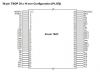
Pinout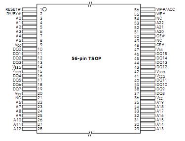 SpecificationsStorage Temperature Plastic Packages . . . . . . . . . . . . 65°C to +150°C
Ambient Temperature with Power Applied . . . . . . . . . . 65°C to +125°C
Voltage with Respect to Ground
VCC (Note 1) . . . . . . . . . . . . . . . . . . . . . . . . . . . . . . . . . . .0.5 V to +4.0 V
A9, OE#, and RESET# (Note 2) . . . . . . . . . . . . . . . . . . . . 0.5 V to +13.0 V
WP#/ACC (Note 2) . . . . . . . . . . . . . . . . . . . . . . . . . . . . . .0.5 V to +10.5 V
All other pins (Note 1) . . . . . . . . . . . . . . . . . . . . . . . . 0.5 V to VCC +0.5 V
Output Short Circuit Current (Note 3). . . . . . . . . . . . . . . . . . . . . . . . 200 mADescriptionThe S29PL032J is a 128/128/64/32 Mbit, 3.0 volt-only PageMode and Simultaneous Read/Write Flash memory device organized as 8/8/4/2Mwords. The S29PL032J are offered in the following packages: 11mm x 8mm, 80-ball Fine-pitch BGA standalone (PL127J and PL129J) 8mm x 11.6mm, 64-ball Fine-pitch BGA multi-chip compatible(PL127J/PL129J) 8.15mm x 6.15mm, 48-ball Fine-pitch BGA standalone (PL064J/PL032J) 7mm x 9mm, 56-ball Fine-pitch BGA multi-chip compatible (PL064J andPL032J) 20mm x 14mm, 56-pin TSOP (PL127J)
The word-wide data (x16) of S29PL032J appears on DQ15-DQ0. This device can be pro-grammed in-system or in standard EPROM programmers. A 12.0 V VPP is notrequired for write or erase operations.
The S29PL032J offers fast page access times of 20 to 30 ns, with corresponding ran-dom access times of 55 to 70 ns, respectively, allowing high speedmicroprocessors to operate without wait states. To eliminate bus contention thedevice has separate chip enable (CE#), write enable (WE#) and output enable(OE#) controls. Note: Device PL129J has 2 chip enable inputs (CE1#, CE2#).

 S29PL032J Data Sheet