Features: Architecture
` Little-/Big-endian support for external memory.
` Address space: 32Mbytes per each bank (Total 256Mbyte)
` Supports programmable 8/16/32-bit data bus width for each memory bank
` Fixed bank start address for all (static memory and dynamic memory banks)
` 8 memory banks
4 memory banks for static memory (ROM, SRAM, FLASH etc)
4 memory banks for dynamic memory (Fast Page, EDO, and Synchronous DRAM)
` Fully programmable access cycles for all static memory banks
` Supports external wait signal to extend the bus cycle
` Supports self-refresh mode in DRAM/SDRAM.
` Supports asymmetric/symmetric address of DRAM
I/D (Instruction/Data) Cache Memory
` 64-way set-associative ICache (16KB) and DCache (16KB)
` 8 words per line with one valid bit and 2 dirty bits per line
` Pseudo-random or round-robin replacement algorithm
` Write-through and Write-back cache operation.
` The write buffer can hold 16 words of data and 4 addresses
` Low voltage cache for reduced power consumption
Clock & Power Manager
` The on-chip PLL generates the necessary clock for the operation of MCU at maximum of 200MHz@1.8V
` Input frequency range: (Fin) = 6MHz 10MHz.
` Output frequency range: (FCLK) = 20MHz 200MHz
` Clock can be selectively provided to each function block by software
` Power Down Mode: NORMAL, SLOW, and IDLE mode
NORMAL mode: Normal operating mode
SLOW mode: Low frequency clock without PLL
IDLE mode: Clock to CPU is disabled
PCI Bus Interface
` Embedded PCI Host Bridge
` 32-bit data bus at 66MHz
Interrupt Controller
` 34 Interrupt sources. (3 for Timers, 6 for UART, 8 for External interrupts, 4 for DMA, 2 for RTC, 2 for IIC, 2 for
RCSR (Remote Control Signal Receiver), and 7 for PCI))
` Software polling Interrupt mode
` Selectable level- or edge-triggered external interrupts source
` Programmable IRQ/FIQ for each interrupt request
` Supports FIQ (Fast Interrupt Request) for very urgent interrupt request
Timer
` 3-ch 16-bit Timer with DMA-based or interruptbased operation
Watchdog Timer
` 16-bit Watchdog Timer
RCSR (Remote Control Signal Receiver)
` 8-step FIFO
` FIFO interrupt is generated on full (8) step overflow
RTC (Real Time Clock)
` Full clock feature: sec, min, hour, date, day, week, month, and year
` 32.768 kHz input clock
` Alarm interrupt
` Time tick interrupt
GPIO (General-Purpose Input/Output) Ports
` 8 external interrupt ports
` 44 multiplexed input/output ports.
UART
` 2-channel UART with DMA-based or interrupt based operation
` Supports 5-bit, 6-bit, 7-bit, or 8-bit serial data transmit/receive
` Supports hardware handshaking during transmit/receive operation
` Programmable baud rates (up to 230.4Kbps).
` Supports IrDA 1.0 (up to 115.2Kbps)
` Loop back mode for testing
` Program accessible 16-byte FIFO (2x16 byte FIFO for transmit/receive data)
DMA Controller
` 4-channel general-purpose Direct Memory Access controller without CPU intervention.
` Support memory to memory, memory to I/O and I/O to I/O DMA operations of the following 6 types: Software,
3 internal function blocks (UART0, UART1, Timer), and 2 External requests
` Burst transfer mode to enhance the transfer rate on the FPDRAM, EDODRAM and SDRAM
IIC-BUS Interface
` 2-ch Multi-Master IIC-Bus with interrupt-based operation
` Serial, 8-bit oriented, bi-directional data transfers at up to 100 Kbit/s in the standard mode or up to 400 Kbit/s
in the fast mode
Operating Voltage Range
` Core: 1.8 V -0.1 V/+0.15 V
` I/O: 3.3 V ± 0.3 V
Operating Frequency
` Up to 200 MHz.
Package
` 208-pin LQFP
Pinout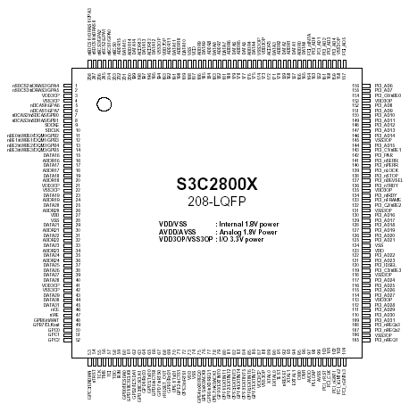 Specifications
|
Symbol |
Parameter |
Rating |
Unit |
|
VDD |
1.8V Core DC Supply Voltage |
2.4 |
V |
|
VDDP |
3.3V I/O DC Supply Voltage |
3.8 |
V |
|
VIN |
DC Input Voltage |
3.3V input buffer |
3.8 |
V |
|
VOUT |
DC Output Voltage |
3.3V Output buffer |
3.8 |
V |
|
ILATCH |
Latch-up current |
± 200 |
|
mA |
|
TSTG |
Storage Temperature |
65 to 150 |
|
|
DescriptionSAMSUNG's S3C2800 32-bit RISC microprocessor is designed to provide a cost-effective and high-performance micro-controller solution for general applications. The S3C2800 features the following integrated on-chip support to help design a system a low cost: 16KB I/D caches, 2-ch UART with handshake, 4-ch DMA, memory controller, 3-ch timer, GPIO (General-Purpose Input/Output) ports, RTC (Real Time Clock), 2-ch IIC-BUS interface, and a built-in PLL for system clock.
Based on ARM920T core, the S3C2800 is developed using 0.18 um CMOS standard cells and a memory compiler. Its simple, elegant, and fully static low-power design is particularly suitable for both cost-sensitive and power-sensitive applications. The 32-bit ARM920T RISC processor core (220Mips @200MHz), designed by Advanced RISC Machines, Ltd., provides architectural enhancements such as the Thumb de-compressor, a 32- bit hardware multiplier, and an on-chip ICE debug support. Also, the S3C2800 features the Harvard BUS architecture for efficient data/instruction transfers.
By integrating various common system peripherals, the S3C2800 minimizes the overall system cost and eliminates the need to configure additional components. The integrated on-chip S3C2800 functions are summarized as follows :
· PCI BUS interface (32-bit, up to 66MHz).
· 1.8V static ARM920T CPU core with 16KB I/D (Instruction/Data) cache. (Harvard bus architecture up to 200MHz).
· External memory controller. (FP/EDO/SDRAM control, Chip select logic).
· 4-ch general DMAs with external request pins.
· 2-ch UART with handshake (IRDA1.0, 16-byte FIFO), Modem Interface.
· 2-ch multi-master IIC-BUS controller.
· 3-ch 16-bit timer.
· 16-bit Watchdog timer.
· 44 general-purpose GPIO ports including 8 external interrupt source.
· Power management: Normal, Slow, and Idle modes.
· RTC with calendar function.
· On-chip PLL clock generator.

 S3C2800 Data Sheet