S3C3410X

Features: Architecture`Integrated system for hand-held and general embedded application.`Fully 16/32-bit RISC architecture(32-bit ARM instruction as well as 16-bit Thumb instruction).`ARM7TDMI CPU core, supporting the efficient and powerful instruction set.`On-chip ICEBreakerTM debug support by JT...

product image

S3C3410X Picture
SeekIC No. : 004482082 Detail

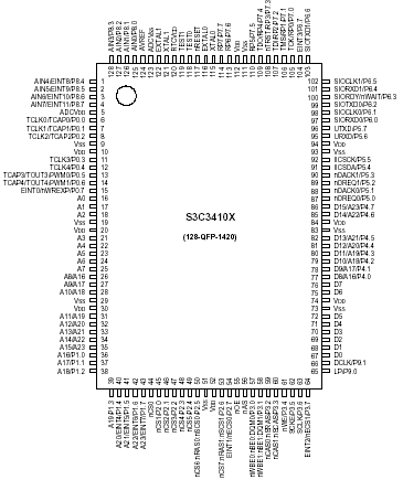
S3C3410X: Features: Architecture`Integrated system for hand-held and general embedded application.`Fully 16/32-bit RISC architecture(32-bit ARM instruction as well as 16-bit Thumb instruction).`ARM7TDMI CPU c...

floor Price/Ceiling Price

Part Number:
S3C3410X
Supply Ability:
5000

Price Break

  • Qty
  • 1~5000
  • Unit Price
  • Negotiable
  • Processing time
  • 15 Days
Total Cost: $ 0.00

SeekIC Buyer Protection PLUS - newly updated for 2013!

  • Escrow Protection.
  • Guaranteed refunds.
  • Secure payments.
  • Learn more >>

Month Sales

268 Transactions

Rating

evaluate  (4.8 stars)

Upload time: 2025/12/26

Payment Methods

All payment methods are secure and covered by SeekIC Buyer Protection PLUS.

Notice: When you place an order, your payment is made to SeekIC and not to your seller. SeekIC only pays the seller after confirming you have received your order. We will also never share your payment details with your seller.
Product Details

Description


Features:

Architecture
`Integrated system for hand-held and general embedded application.
`Fully 16/32-bit RISC architecture(32-bit ARM instruction as well as 16-bit Thumb instruction).
`ARM7TDMI CPU core, supporting the efficient and powerful instruction set.
`On-chip ICEBreakerTM debug support by JTAGbased solution.
`4KB Unified Cache (Instruction/Data Cache Memory)

System Manager
` Address space: 16Mbytes per each bank (Total 128Mbyte)
` Support 8-bit/16-bit data bus width for external memory/device access.
` The bank can support ROM/SRAM/Flash, External I/O device or FP/EDO/SDRAM.
` Among total 8 memory banks, bank0,1,2,3,4 and 5 can be mapped to ROM/SRAM/Flash, while bank6 and 7
   can be mapped to FP/EDO/SDRAM as well as ROM/SRAM/Flash.
` Fully programmable access cycle for all memory banks
` Supports self-refresh/auto-refresh mode to retain the data in the DRAM.
` Two external I/O banks can be mapped to the SFR (Special Function Register) region.

Unified(Instruction/Data) Cache Memory & Internal SRAM
` Two-way set associative 4KB cache.
` Pseudo LRU (Least Recently Used) replacement policy.
` Four depth write buffer.
` Programmable configuration of (4KB cache, only), (2KB cache and 2KB SRAM), or (4KB SRAM, only).

DMA Controller
` Two-channel general purposed DMA(Direct Memory Access) controller.
` The data transfer of Memory-to-memory, serial port-to-memory, memory-to-serial port, memoryto- SFR(
    Special Function Register), SFR-tomemory, internal SRAM-to-memory, and memory-to-internal SRAM without
   CPU intervention
` Initiated by the software or external DMA request
` Increment or decrement source or destination addresses.
` Supports 8-bit(byte), 16-bit(half-word), and 32- bit(word) of data transfer size.

I/O Ports
` 10 Programmable Input, Output, and I/O port group (74 I/O ports including the multiplexed I/O)
` One programmable Output port (2-bit multiplexed output ports)
` One programmable Input port(8-bit multiplexed input ports)
` Eight programmable I/O port group. 16-bit Timer/Counters (T0, T1, T2)
` Three-channel programmable 16-bit timer/counter
` Interval, capture, match & overflow, or DMA mode operation
` Internal or external clock source

8-bit Timer/Counters (T3, T4)
` Two-channel programmable 8-bit timer/counter
` Interval, capture, PWM, or DMA mode operation (T4 PWM with 5-byte FIFO buffer, which can provide the
   sound generation capability)
` Internal or external clock source

UART & SIO
` One-channel UART with DMA-based or interrupt-based operation
` Programmable baud rates
` Supports 5-bit, 6-bit, 7-bit and 8-bit serial data transmit/receive frame in UART
` Programmable accessible 8-byte transmitter FIFO and 8-byte receiver FIFO in UART
` Two-channel synchronous SIO with DMA-based or interrupt-based operation
` Support the serial data transmit/receive operation by 8-bit frame.

Interrupt Controller
` 35 interrupt sources (12 External interrupt, 2 DMA, 3 UART, 11 Timer, ADC, IIC, 2 SIO, Basic Timer, 2 RTC)
` H/W interrupt priority logic and vector generation
` Normal or fast interrupt modes (IRQ, FIQ)

A/D Converter
` Eight-channel multiplexed ADC
` Successive approximation conversion
` 10-bit ADC

WDT(Watch-Dog Timer) and Basic Timer
` 8-bit Counter (Basic Timer) and 3-bit counter (Watchdog Timer)
` The overflow signal of 8-bit counter can generate a basic timer interrupt and should be input clock for 3-bit
    counter(Watchdog Timer).
` The overflow signal of 3-bit counter makes a system reset

IIC Bus Interface
` One-channel multi-master IIC-bus
` Support 8-bit, bi-directional, and serial data transfer up to 100kbit/s.

RTC (Real Time Clock)
` Full clock function : second, minute, hours, day, wek, month, and year
` 32.768KHz operation
` Alarm interrupt for CPU wake-up

Power Down Mode
` Power mode: Idle, Slow and Stop mode
` System clock division ratio in slow mode: 1, 1/2, 1/8, 1/16, and 1/1024

Operating Voltage Range
` 3.0 V to 3.6 V

Temperature Range
` 0 to 70

Operating Frequency
` up to 40MHz

Package Type
` 128-pin QFP


Pinout

  Connection Diagram


Specifications

Symbol
Parameter
Rating
Unit
VDD
DC Supply Voltage
0.3 to 3.8
V
VIN
DC Input Voltage
0.3 to VDD + 0.3
V
IIN
DC Input Current
± 10
mA
TA
Operating Temperature
0 to 70
TSTG
Storage Temperature
40 to 125
RTCVDD
Battery Voltage for RTC
2.5 to VDD
V


Description

Samsung's S3C3410X 16/32-bit RISC microcontroller is a cost-effective and high-performance microcontroller solution for PDA and general purpose application.

An outstanding feature of the S3C3410X is its CPU core, a 16/32-bit RISC processor(ARM7TDMI) designed by Advanced RISC Machines, Ltd. The ARM7TDMI core is a low-power, general purpose, microprocessor macrocell, which was developed for the use in application-specific and customer-specific integrated circuits. Its simple, elegant, and fully static design is particularly suitable for cost-sensitive and power-sensitive application.

The S3C3410X has been developed by using the ARM7TDMI core, CMOS standard cell, and a data path compiler. Most of the on-chip function blocks have been designed using an HDL synthesizer. The S3C3410X has been fully verified in SAMSUNG ASIC test environment including the internal Qualification Assurance Process.

By providing a complete set of common system peripherals, the S3C3410X can minimize the overall system cost and eliminates the need to configure additional components, externally.

The integrated on-chip S3C3410X functions which are described in this document include:

·  Integrated external memory controller (ROM/SRAM and FP/EDO DRAM/SDRAM controller)
·  2-channel general DMA controller
·  Internal 4K-byte memory can be configured as (4KB Cache only), (2KB Cache and 2KB SRAM), or (4KB SRAM only).
·  1-channel UART with IrDA 1.0, 1-channel IIC, and 2-channel SIO(Synchronous serial IO)
·  3-channel 16-bit timers and 2-channel 8-bit timers
·  Real time clock with calendar function.
·  Crystal/Ceramic oscillator or external clock can be used as the clock source.
·  Power control: Normal, Idle, and Stop mode
·  1-channel 8-bit basic timer and 3-bit watch-dog timer
·  Interrupt controller: 35 interrupt sources, interrupt priority control logic and interrupt vector generation by H/W.
·  8-channel 10-bit ADC
·  10 programmable I/O port group (Total 74 I/O ports including the multiplexed I/O)


Customers Who Bought This Item Also Bought

Margin,quality,low-cost products with low minimum orders. Secure your online payments with SeekIC Buyer Protection.
Fans, Thermal Management
Crystals and Oscillators
Potentiometers, Variable Resistors
LED Products
View more