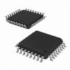
S9S08AW8A

Features: MC9S08AC16 Series Devices• Consumer & Industrial- MC9S08AC16- MC9S08AC8• Automotive- S9S08AW16A- S9S08AW8A8-Bit HCS08 Central Processor Unit (CPU)• 40-MHz HCS08 CPU (central processor unit)• 20-MHz internal bus frequency• HC08 instruction set with added ...

product image

S9S08AW8A Picture
SeekIC No. : 004483496 Detail

S9S08AW8A: Features: MC9S08AC16 Series Devices• Consumer & Industrial- MC9S08AC16- MC9S08AC8• Automotive- S9S08AW16A- S9S08AW8A8-Bit HCS08 Central Processor Unit (CPU)• 40-MHz HCS08 CPU (...

floor Price/Ceiling Price

Part Number:
S9S08AW8A
Supply Ability:
5000

Price Break

  • Qty
  • 1~5000
  • Unit Price
  • Negotiable
  • Processing time
  • 15 Days
Total Cost: $ 0.00

SeekIC Buyer Protection PLUS - newly updated for 2013!

  • Escrow Protection.
  • Guaranteed refunds.
  • Secure payments.
  • Learn more >>

Month Sales

268 Transactions

Rating

evaluate  (4.8 stars)

Upload time: 2024/4/27

Payment Methods

All payment methods are secure and covered by SeekIC Buyer Protection PLUS.

Notice: When you place an order, your payment is made to SeekIC and not to your seller. SeekIC only pays the seller after confirming you have received your order. We will also never share your payment details with your seller.
Product Details

Description


Features:

MC9S08AC16 Series Devices
• Consumer & Industrial
- MC9S08AC16
- MC9S08AC8
• Automotive
- S9S08AW16A
- S9S08AW8A
8-Bit HCS08 Central Processor Unit (CPU)
• 40-MHz HCS08 CPU (central processor unit)
• 20-MHz internal bus frequency
• HC08 instruction set with added BGND instruction
• Background debugging system
• Breakpoint capability to allow single breakpoint setting during in-circuit debugging (plus two more breakpoints in on-chip debug module)
• Debug module containing two comparators and nine trigger modes. Eight deep FIFO for storing change-of-flow addresses and event-only data. Debug module supports both tag and force breakpoints.
• Support for up to 32 interrupt/reset sources Memory Options
• Up to 16 KB of on-chip in-circuit programmable FLASH memory with block protection and security options
• Up to 1 KB of on-chip RAM Clock Source Options
• Clock source options include crystal, resonator, external clock, or internally generated clock with precision NVM trimming System Protection
• Optional computer operating properly (COP) reset with option to run from independent internal clock source or bus clock
• Low-voltage detection with reset or interrupt
• Illegal opcode detection with reset
• Illegal address detection with reset Power-Saving Modes
• Wait plus two stops Peripherals
• ADC - 8-channel, 10-bit analog-to-digital converter with automatic compare function
• SCI - Two serial communications interface modules with optional 13-bit break
• SPI - Serial peripheral interface module
• IIC - Inter-integrated circuit bus module to operate at up to 100 kbps with maximum bus loading; capable of higher baud rates with reduced loading
• Timers - Three1 16-bit timer/pulse-width modulator (TPM) modules - Two1 2-channel and one 4-channel; each has selectable input capture, output compare, and edge-aligned PWM capability on each channel. Each timer module may be configured for buffered, centered PWM (CPWM) on all channels
• KBI - 7-pin keyboard interrupt module Input/Output
• Up to 38 general-purpose input/output (I/O) pins
• Software selectable pullups on ports when used as inputs
• Software selectable slew rate control on ports when used as outputs
• Software selectable drive strength on ports when used as outputs
• Master reset pin and power-on reset (POR)
• Internal pullup on RESET, IRQ, and BKGD/MS pins to reduce customer system cost Package Options
• 48-pin quad flat no-lead package (QFN)
• 44-pin low-profile quad flat package (LQFP)
• 32-pin low-profile quad flat package (LQFP)


Specifications

Rating Symbol Value Unit
Supply voltage VDD 0.3 to + 5.8 V
Input voltage VIn 0.3 to VDD + 0.3 V
Instantaneous maximum current
Single pin limit (applies to all port pins)1, 2, 3
ID ± 25 mA
Maximum current into VDD IDD 120 mA
Storage temperature Tstg 55 to +150
Maximum junction temperature TJ 150

1 Input must be current limited to the value specified. To determine the value of the required current-limiting resistor, calculate resistance values for positive (VDD) and negative (VSS) clamp voltages, then use the larger of the two resistance values.

2 All functional non-supply pins are internally clamped to VSS and VDD.

3 Power supply must maintain regulation within operating VDD range during instantaneous and operating maximum current conditions. If positive injection current (VIn > VDD) is greater than IDD, the injection current may flow out of VDD and could result in external power supply going out of regulation. Ensure external VDD load will shunt current greater than maximum injection current. This will be the greatest risk when the MCU is not consuming power. Examples are: if no system clock is present, or if the clock rate is very low which would reduce overall power consumption.


Description

The oscillator pins are used to provide an external clock source for the MCU. The oscillator pins S9S08AW8A are gain controlled in low-power mode (default). Oscillator amplitudes in low-power mode are limited to approximately 1 V, peak-to-peak.


Customers Who Bought This Item Also Bought

Margin,quality,low-cost products with low minimum orders. Secure your online payments with SeekIC Buyer Protection.
Sensors, Transducers
Soldering, Desoldering, Rework Products
Cable Assemblies
Transformers
Semiconductor Modules
View more