DescriptionThe SC11372 is designed as a CMOS integrated circuit for performing the baseband signal processing for multi-standard mobile radio applications. Application of the IC will allow equipment makers to use the same baseband circuitry in a range of PMR products and therefore reduce device in...
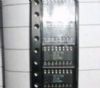
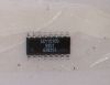
SC11372: DescriptionThe SC11372 is designed as a CMOS integrated circuit for performing the baseband signal processing for multi-standard mobile radio applications. Application of the IC will allow equipment...
SeekIC Buyer Protection PLUS - newly updated for 2013!
268 Transactions
All payment methods are secure and covered by SeekIC Buyer Protection PLUS.
The SC11372 is designed as a CMOS integrated circuit for performing the baseband signal processing for multi-standard mobile radio applications. Application of the IC will allow equipment makers to use the same baseband circuitry in a range of PMR products and therefore reduce device inventory.
It has twelve features. (1)All receive and transmit filtering plus gain control for hlaf duplex audio communications. (2)Automatic level control. (3)DTMF transmitter. (4)Programmable clock generator with CPU output. (5)8-bit DAC output. (6)I2C bus interface. (7)6/8-bit ADC on board. (8)CTCSS transceiver. (9)SELCALL transceiver. (10)NRZ sub-audio transceiver for DCS systems. (11)Low power 5V CMOS. (12)FFSK 12/400 modem. Those are all the main features.
Some absolute maximum ratings have been concluded into several points as follow. (1)Its power supply voltage would be max 6V. (2)Its voltage on any pin would be min Vss-0.3V and max Vdd+0.3V. (3)Its current at any pin would be max 10mA. (4)Its storage temperature range would be from -65°C to 150°C. (5)Its package power dissipation would be 500mW at 25°C. It should be noted that stresses above those listed in absolute maximum ratings may cause permanent damage to device.
Also some electrical characteristics are concluded as follow. (1)Its digital high level would be min 0.7Vdd. (2)Its digital low level would be max 0.3Vdd. (3)Its sleep mode current would be typ 950uA and max 1200uA. (4)Its min active mode current would be typ 1550uA and max 1900uA. (5)Its max supply current would be typ 14.5mA. (6)Its positive supply voltage would be min 4.75V and typ 5V and max 5.25V. (7)Its frequency at XIN pin would be typ 1.0592MHz. And so on. At present we have got so much information about this IC and we would try hard to get more information about it. If you have any question or suggestion or want to know more information please contact us for details. Thank you!