DescriptionThe SC1485ITSTR is designed as a dual output constant on synchronous buck PWM controller intended for use in notebook computers and other battery operated portable devices. Features include high efficiency and a fast dynamic response with no minimum on time. The excellent transient resp...
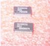
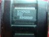
SC1485ITSTR: DescriptionThe SC1485ITSTR is designed as a dual output constant on synchronous buck PWM controller intended for use in notebook computers and other battery operated portable devices. Features inclu...
SeekIC Buyer Protection PLUS - newly updated for 2013!
268 Transactions
All payment methods are secure and covered by SeekIC Buyer Protection PLUS.
The SC1485ITSTR is designed as a dual output constant on synchronous buck PWM controller intended for use in notebook computers and other battery operated portable devices. Features include high efficiency and a fast dynamic response with no minimum on time. The excellent transient response, means that it based solutions will require less output capacitance than competing fixed frequency converters.
SC1485ITSTR has many features. (1)Constant on-time for fast dynamic response. (2)Programmable Vo range is 0.5V to Vcca. (3)Win range is 1.8V to 25V. (4)DC current sense using low-side Rds(on) sensing or sense resistor. (5)Resistor programmable frequency. (6)Cycle-by-cycle current limit. (7)Digital soft-start. (8)Separate PSAVE option for each switcher. (9)Over-voltage/under voltage fault protection. (10)10uA typical shutdown current. (11)Low quiescent power dissipation. (12)Two PGOOD indicators. (13)1% reference (2% system DC accuracy). (14)Efficiency>90%. And so on.
Some absolute maximum ratings of SC1485ITSTR have been concluded into several points as follow. (1)Its Ton1 to AGND1, Ton2 to AGND2 would be from -0.3V to 25V. (2)Its DH1, BST1 to AGND1 and DH2, BST2 to AGND2 would be from -0.3v to 30V. (3)Its LX1 to AGND1 and LX2 to AGND2 would be from -2.0V to 25V. (4)Its AGND1 to PGND1 and AGND2 to PGND2 would be from -0.3V to 0.3V. (5)Its BST1 to LX1 and BST2 to LX2 would be from -0.3V to 6V. (6)Its Vcca1, PGOOD1, EN/PSV1, ILIM1, Vout1, DL1 to PGND1 would be from -0.3V to 6.0V. (7)Its thermal resistance junction to ambient would be 37°C/W. (8)Its operating junction temperature range would be from -40°C to 125°C. (9)Its storage temperature range would be from -65°C to 150°C. (10)Its lead temperature soldering 10 seconds would be 300°C. It should be noted that stresses above those listed in absolute maximum ratings may cause permanent damage to device. And so on. If you have any question or suggestion or want to know more information please contact us for details. Thank you!