SCAN18540T

Features: IEEE 1149.1 (JTAG) compliant Dual output enable signals per byte TRI-STATE outputs for bus-oriented applications 9-bit data busses for parity applications Reduced-swing outputs source 24 mA/sink 48 mA (Mil) Guaranteed to drive 50 transmission line to TTL input levels of 0.8V and 2.0V TT...

product image

SCAN18540T Picture
SeekIC No. : 004485830 Detail

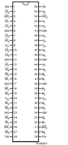
SCAN18540T: Features: IEEE 1149.1 (JTAG) compliant Dual output enable signals per byte TRI-STATE outputs for bus-oriented applications 9-bit data busses for parity applications Reduced-swing outputs source 24 ...

floor Price/Ceiling Price

Part Number:
SCAN18540T
Supply Ability:
5000

Price Break

  • Qty
  • 1~5000
  • Unit Price
  • Negotiable
  • Processing time
  • 15 Days
Total Cost: $ 0.00

SeekIC Buyer Protection PLUS - newly updated for 2013!

  • Escrow Protection.
  • Guaranteed refunds.
  • Secure payments.
  • Learn more >>

Month Sales

268 Transactions

Rating

evaluate  (4.8 stars)

Upload time: 2026/1/20

Payment Methods

All payment methods are secure and covered by SeekIC Buyer Protection PLUS.

Notice: When you place an order, your payment is made to SeekIC and not to your seller. SeekIC only pays the seller after confirming you have received your order. We will also never share your payment details with your seller.
Product Details

Description


Features:

IEEE 1149.1 (JTAG) compliant
Dual output enable signals per byte
TRI-STATE outputs for bus-oriented applications
9-bit data busses for parity applications
Reduced-swing outputs source 24 mA/sink 48 mA (Mil)
Guaranteed to drive 50 transmission line to TTL input levels of 0.8V and 2.0V
TTL compatible inputs
25 mil pitch Cerpack packaging
Includes CLAMP and HIGHZ instructions
Standard Microcircuit Drawing (SMD) 5962-9312701


Pinout

  Connection Diagram


Specifications

If Military/Aerospace specified devices are required, please contact the National Semiconductor Sales Office/Distributors for availability and specifications.
Supply Voltage (VCC)                                                             −0.5V to +7.0V
DC Input Diode Current (IIK)
VI = −0.5V                                                                             −20 mA
VI = VCC +0.5V                                                                      +20 mA
DC Output Diode Current (IOK)
VO = −0.5V                                                                            −20 mA
VO = VCC +0.5V                                                                     +20 mA
DC Output Voltage (VO)                                                         −0.5V to VCC +0.5V
DC Output Source/Sink Current (IO)                                     ±70 mA
DC VCC or Ground Current
Per Output Pin                                                                      ±70 mA
Junction Temperature
Cerpack                                                                                +175°C
Storage Temperature                                                           −65°C to +150°C
ESD (Min)                                                                              2000V


Description

The SCAN18540T is a high speed, low-power line driver featuring separate data inputs organized into dual 9-bit bytes with byte-oriented paired output enable control signals. This SCAN18540T is compliant with IEEE 1149.1 Standard Test Access Port and Boundary Scan Architecture with the incorporation of the defined boundary-scan test logic and test access port consisting of Test Data Input (TDI), Test Data Out (TDO), Test Mode Select (TMS), and Test Clock (TCK).


Customers Who Bought This Item Also Bought

Margin,quality,low-cost products with low minimum orders. Secure your online payments with SeekIC Buyer Protection.
Memory Cards, Modules
Potentiometers, Variable Resistors
Batteries, Chargers, Holders
Integrated Circuits (ICs)
Soldering, Desoldering, Rework Products
View more